Diffraction
advertisement
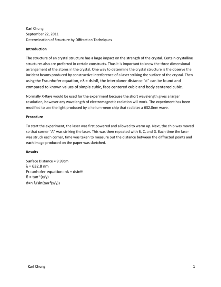
Karl Chung September 22, 2011 Determination of Structure by Diffraction Techniques Introduction The structure of an crystal structure has a large impact on the strength of the crystal. Certain crystalline structures also are preferred in certain constructs. Thus it is important to know the three dimensional arrangement of the atoms in the crystal. One way to determine the crystal structure is the observe the incident beams produced by constructive interference of a laser striking the surface of the crystal. Then using the Fraunhofer equation, nλ = dsinθ, the interplaner distance “d” can be found and compared to known values of simple cubic, face centered cubic and body centered cubic. Normally X-Rays would be used for the experiment because the short wavelength gives a larger resolution, however any wavelength of electromagnetic radiation will work. The experiment has been modified to use the light produced by a helium-neon chip that radiates a 632.8nm wave. Procedure To start the experiment, the laser was first powered and allowed to warm up. Next, the chip was moved so that corner “A” was striking the laser. This was then repeated with B, C, and D. Each time the laser was struck each corner, time was taken to measure out the distance between the diffracted points and each image produced on the paper was sketched. Results Surface Distance = 9.99cm λ = 632.8 nm Fraunhofer equation: nλ = dsinθ θ = tan-1(x/y) d=n λ/sin(tan-1(x/y)) Karl Chung 1 A. Image produced was symmetric on Y and X axis. The Vertical distance measured from origin was 10cm and the horizontal was 8cm. B. Symmetric about Y and X axis. Distance between all the points was 3.75cm. C. Symmetric about X axis. Distance from origin is 8cm D. Symmetric about X and Y. Distance from origin is 8.25 cm Karl Chung Sample x (mm) θ (degrees) d (nm) A 80 38.68 1019 100 45.028 894.477 B 37.5 20.57 1801 C 80 38.68 1012 D 8.25 39.55 993.79 2 Discussion The results of the distances, d, correspond to each of the etchings on the chips for each corner. The angle theta used in the equation was calculated by the arctan of the higher, 99.9mm divided by the horizontal distance x measured for each chip. All of the values were then used in the equation for “d” described above. By experimental method, chip A had two different distances, each of which were 1019 and 894nm apart accordingly. B had a spacing distance of 1801nm and C had a spacing of 1012. D had a spacing of 993.79. A,B, and D all had two dimensional arrays because the dots were in two dimensional space on the chip. Corner C had only a one dimensional array because the lines on the chip were only in one dimension. Conclusion The modified Braggs law was used to measure the etching distance on each chip. The lab was a modified version of the x-ray diffraction technique used to find the structure arrangement of atoms in a solid. Instead it found the spacing between the etchings. Diffraction techniques are very useful for finding understand the structure of crystals. References MATERIALS SCIENCE FOR ENGINEERS LABORATORY MANUAL FALL 2005 Messler, Robert W. The Essence of Materials for Engineers. Sudbury, MA: Jones and Bartlett Learning, 2011. Print. Karl Chung 3

