Manufacturing of the passive electronic components
advertisement

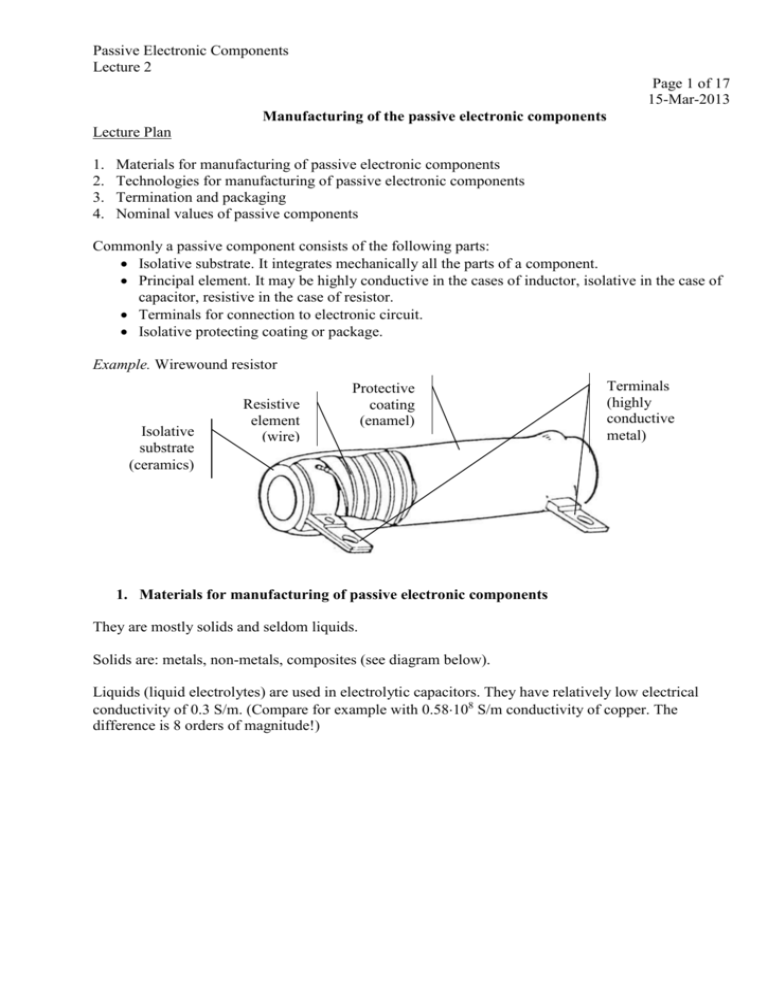
Passive Electronic Components Lecture 2 Page 1 of 17 15-Mar-2013 Manufacturing of the passive electronic components Lecture Plan 1. 2. 3. 4. Materials for manufacturing of passive electronic components Technologies for manufacturing of passive electronic components Termination and packaging Nominal values of passive components Commonly a passive component consists of the following parts: Isolative substrate. It integrates mechanically all the parts of a component. Principal element. It may be highly conductive in the cases of inductor, isolative in the case of capacitor, resistive in the case of resistor. Terminals for connection to electronic circuit. Isolative protecting coating or package. Example. Wirewound resistor Isolative substrate (ceramics) Resistive element (wire) Protective coating (enamel) Terminals (highly conductive metal) 1. Materials for manufacturing of passive electronic components They are mostly solids and seldom liquids. Solids are: metals, non-metals, composites (see diagram below). Liquids (liquid electrolytes) are used in electrolytic capacitors. They have relatively low electrical conductivity of 0.3 S/m. (Compare for example with 0.58108 S/m conductivity of copper. The difference is 8 orders of magnitude!) Passive Electronic Components Lecture 2 Page 2 of 17 Solid materials in passive components Metals Non-metals Elemental metals Ceramics Alloys Polymers Composites Intermetallic compounds 1.1. Metals (Elemental metals. Alloys. Intermetallic compounds). Metal is an element, alloy, or compound that is a good conductor of both electricity and heat. Metals are usually malleable and shiny (reflect most of incident light). Atoms in a metal readily lose electrons forming positive ions (cations). Thermal conductivity of the metals is provided mainly by the same free electrons that ensure electrical conductivity. Particular part of thermal conductivity in metals is related to oscillations of atoms in the lattice. The atoms in any solid are always in a state of vibration. Their average kinetic energy is measured by the absolute temperature of the solid. Relative electrical and thermal conductivities of some metals (conductivities of copper are supposed to be equal to 100 units) Electrical Thermal 120 100 80 60 40 20 ry er cu M ad Ti ta ni um Le Ti n Ir o n Pa lla di um Pl at in iu m el iu m Li th N ic k Zi nc en st Tu ng in iu m G ol d Al um pe r C op Si lv er 0 Passive Electronic Components Lecture 2 Page 3 of 17 Elemental metals (pure metals) like silver (Ag), copper (Cu), gold (Au), aluminum (Al), iron (Fe), tin (Sn). Silver is the best electrical and thermal conductor among all the metals. Copper takes the second place (see graph above). The drawbacks of silver are: 1) Remarkable susceptibility to electromigration – electrochemical process of dendrite crystal growth between metal electrodes in the presence of (a) electrical potential difference, (b) humidity, (c) ionic contamination. The dendrites may result in short circuit. 2) Remarkable susceptibility to sulfuration (chemical reaction with sulfur and some of its compounds) resulting in transforming of silver into silver sulfide and electrical conductivity loss. This failure mode is typical for automotive electronics because engine exhaust gas comprises sulfur compounds. Alloys. An alloy is a mixture or solid solution composed of two or more elements of which at least one is a metal. The examples of alloy are steel, nichrome, brass, solders. Alloy always is worse electrical and thermal conductor than at least one elemental metal that it is composed of. Intermetallic compounds. Metallic elements may form chemical compounds which are called intermetallic compounds or intermetallics. For example Cu6Sn5 and Cu3Sn compounds are formed as a result of mutual diffusion of copper and tin in copper/tin interface of soldered copper parts. Thin intermetallic layer ensure good adhesion between copper and solder. Thick intermetallic layer may result in solder joint cracking. The main applications of metals in passive components are: terminals (in all kinds of components); resistive elements; capacitor electrodes; inductor windings; fusing elements in fuses. 1.2. Non-metals (Ceramics. Polymers. Semiconductors). Heat transfer in non-metallic solids is carried out mainly by vibration of atoms (phonons). 1.2.1. Ceramics are non-metallic, inorganic materials. Originally they were considered to be oxides (from the Greek word keramos for burnt clay or pottery). Traditional ceramics are burnt clays. Modern ceramics are oxides, carbides, borides, etc. Certain ceramics are amorphous (non-crystalline). They are termed glasses. Ceramic insulators. Dielectric constant < 30 Electrical resistivity > 1010 m Dielectric strength > 5.0 kV/mm Passive Electronic Components Lecture 2 Page 4 of 17 Thermal Conductivity of Ceramic Materials, @ 273-373K, W/(m*K) 1600 1500 1400 1200 1000 800 Copper 401 W/(mK) 600 400 223 200 170 121 32 0 Diamond BeO AlN SiC Al2O3 (Diamond is Chemical Vapor Deposition (CVD) synthetic diamond). Ceramic conductors with linear resistance. The examples are: PdO, RuO2, Bi2Ru2O7 and Bi2Ir2O7 mixed with a glaze, usually a lead borosilicate of typical composition 52 wt%. They are used in manufacturing of thick-film resistors. Tin oxide (SnO2) and Indium-Tin-Oxide (ITO). Tin oxide is an n-type, wide-band-gap (Eg=3.6 eV) semiconductor. The electrical conductivity of tin oxide results primarily from the existence of oxygen vacancies, which act as donors. ITO film conductivity is (0.1…0.5)106 (m)-1. Important: both SnO2 and ITO are transparent! Applications: metal oxide resistors, liquid crystal displays, capacitive touch screens. Ceramic conductors with linear resistance are used as: resistive elements in resistors: thick-film, thin-film (metal oxide), liquid crystal displays, capacitive touch screens, electrodes in gas sensors, batteries and fuel cells, anodes in niobium capacitors (NbO). (For comparison: Nb2O5 is a dielectric in the same type of capacitors), cathodes in tantalum and niobium capacitors (MnO2). (For comparison: Mn2O3 is a dielectric that forms as a results of MnO2 heating), heating elements. Their main advantages when compared to metallic and metallic-based thickfilm heaters are: (a) full ceramic microstructure which allows operation at the temperatures in access of 1000 °C, (b) ability to work in corrosive medium. Ceramic conductors with non-linear (voltage dependant) resistance are used in: surge suppressors (arresters) – ZnO, NTC and PTC thermistors (most NTC materials are based on solid solutions Fe3O4-ZnCr3O4 and Fe3O4-MgCr2O4), heaters (PTC ceramic conductors like polycrystalline dopped barium titanate BaTiO3, silicon carbide SiC). Passive Electronic Components Lecture 2 Page 5 of 17 High permittivity ferroelectric ceramics Material Dielectric permittivity BaTi4O9 38 TiO2 85 Some high-permittivity ceramics have dielectric permittivity that exceeds 1000. Ferroelectric ceramics are formulated from a number of compositions and solid solutions, including barium titanate, lead zirconate titanate (PZT), lead niobate, bismuth titanate, sodium potassium niobate and lead titanate. Foremost of these has been barium titanate. Applications of piezoelectric materials include: High voltage generators (gas ignitors). Ultrasonic transducers (ultrasonic cleaners, ultrasonic welding). Sounders (loudspeakers, buzzers, alarms). Sensors (phonograph pickups, accelerometers). Resonators (interim frequency filters, surface wave filters, delay lines piezo-transformers). Miscellaneous (relays, pumps, motors, fans, positioners, printers, touch-controls). Magnetic ceramics. Ferrites are the predominant materials for magnetic ceramics. They are based on iron oxides (Fe3O4 is a major component). Applications of ceramics in passive components. electrically isolative and thermally conductive substrates of discrete and integrated resistors, capacitors, inductors (Al2O3, AlN, BeO); dielectric in ceramic capacitors (ferroelectric ceramics); electrodes in electrolytic capacitors (NbO - anode, MnO2 - cathode); resistive elements in film resistors (SnO2, PdO, RuO2); inductor cores (ferrites - Fe3O4); varistors and thermistors (ZnO, Fe3O4-ZnCr3O4). 1.2.2. Polymers (from the Greek, poly- many; meros- part). Polymer molecules are comprised of many simpler molecules (the “mers”) strung together. Polymers are compounds having long chain-like molecules containing carbon-hydrogen bonds. Such compounds are called organic compounds. The example of typical polymer molecule is polyethylene molecule (see below). It can be represented as a long chain of carbon atoms (carbon atom “backbone”) linked to each other. Each carbon atom in turn is linked to two hydrogen atoms. Ethylene (monomer) Polyethylene (polymer) The first polymers were natural products. The example is natural rubber prepared from the Hevea trees that was used by the American Indians when Columbus arrived in 1492. Modification of native Passive Electronic Components Lecture 2 Page 6 of 17 polymers started in the mid-nineteenth century and the first wholly synthetic polymer "Bakelite" was synthesized in 1907. The science of polymers began in the 1920s. Epoxy resins were made in 1936. Another very important class of polymers is silicon polymers. Silicones have an alternating -Si-Otype of “backbone” structure. Silicones are water repellent, heat stable, and very resistant to chemical attack. The segment of silicon molecule is presented below. Silicon (polymer) Polymer isolators. Variety of items are available. They are used for encapsulation of all types of components (the examples are epoxy, polyimide, silicone) and as capacitors dielectric like the following two materials: POLYESTER (MYLAR): A strong material often used in film sheets and tapes for graphic arts and electronics. Those shiny balloons and "space blankets" are usually made from metalized Mylar. Mylar is also used as a dielectric in capacitors. POLYSTYRENE: A clear insulator with superb dielectric properties. Polystyrene capacitors exhibit little dielectric adsorption and virtually no leakage. Liquid polystyrene or Q-dope is a low-loss coil dope used to secure windings and other components in RF circuits. Polymer conductors or conductive polymers. (Do not mix up with metal filled polymers!) In the year 2000 the Nobel Prize in Chemistry was awarded to three men from the field of conductive polymers commonly known as “synthetic metals”. The award was given to Alan J. Heeger, Alan G. MacDiarmid and Hideki Shirakawa. In the early 1970s, Shirakawa synthesized a silvery film, transpolyacetylene, by accidentally adding “a thousand-fold too much catalyst” to the reaction vessel. This mistake gave rise to the invention. Conjugated polymers, also known as conducting polymers, are distinguished by alternating single and double bonds between carbon atoms on the polymer backbone. Acetylene (monomer) Polyacetylene (polymer) Passive Electronic Components Lecture 2 Page 7 of 17 Important application of conductive polymers in the field passive components is an electrolyte (cathode) in electrolyte capacitors. Conductive polymers have significantly higher conductivity than traditional liquid or solid electrolytes. Type of electrolyte Electrolytic solution MnO2 Polymerized organic semiconductor Conductivity, mS/cm 3 30 3,000 Resistivity, mm 3,300 330 3.3 1.2.3. Composites are solid physical mixtures of two or more materials. A composite material may be defined as a combination of at least two chemically and mechanically distinct materials with a definite interface separating the components. Wood and Rock are natural composites, whereas reinforced concrete is a man-made (engineered) composite. A true composite might be considered to have a matrix material completely surrounding its reinforcing material in which the two phases act together to produce characteristics not attainable by either constituent acting alone. Multiphase alloys are not considered composites because their phases are not formed in separate processes but originate in a single manufacturing process. The most important composite materials used in passive components manufacturing are: Cermets – a material consisting of ceramic (glass) and metal particles. Glass makes it possible to bond cermets to ceramic substrate. Thick-film technology is based mainly on these materials. Metal and carbon filled polymers are used for example for interconnections inside tantalum capacitors, for gluing components to PCB, for forming resistors and conductive paths directly on polymer PCB. Molding compounds (epoxy, silicon). Used for packaging of electronic components. Glass-epoxy (FR4, FR5, etc.) are used as PCB substrate (sometimes as component substrate). Soft Magnetic Composites (SMC) is the internationally recognized name for pressed and heat-treated polymer bonded metal powder materials. SMC materials are composed of surfaceinsulated iron powder particles and polymer bonding material. They are used as core materials in inductors. Passive Electronic Components Lecture 2 Page 8 of 17 2. Technologies for manufacturing of passive electronic components 2.1. Bulk elements assembly. The first passive components like wirewound resistor; wirewound inductor; rheostat; paper capacitor; coherer; magnetic detector were manufactured using the available machine building processes: cutting, welding, screwing, molding, gluing, etc. See for example in the pictures below: magnetic detector invented by G. Marconi in 1902 and used in 1903-1918 (left); variable resistor manufactured in Leiden University in 1850 (right). By the way, wirewound resistors, wirewound inductors, capacitors assembled of separate metal and dielectric sheets are used sometimes nowadays. 2.2. Thick-film technology 2.2.1 History of the technique. Screen Printing is a form of stencil printing in which the stencil is adhered to a fine screen (mesh) for support. Ink (paste) can be squeegeed through the screen onto cloth, paper, etc. This technique is also referred to as "silk screen" and "serigraphy". It was known 2000-3000 years ago (Chinese wall print and cloth with multiple layer patterns). In 50’s screen-printed circuitry on ceramic substrate was regarded as replacement of copper clad PCB on polymer-based substrate. Thick-film hybrid circuits (“microcircuits” with screen printed interconnections and resistors) and compatible transistors were developed in the Centralab Division of Globe Union Inc. in Milwaukee. Here in 1947 started his career Jack Kilby, inventor of integrated circuit. In Centralab he dealt with ceramic-based, screen-printed circuits for consumer electronics. In 1967 Dale company (now Vishay-Dale) started development of thick film networks in Columbus (Nebraska, USA). 2.2.2 Equipment: Screen (wire or polymer mesh covered by emulsion), squeegee, printer. Passive Electronic Components Lecture 2 Page 9 of 17 2.2.3 Materials: inks (pastes), substrates. 2.2.4 Types of inks. The adhesion of ink material to ceramic substrate may be provided by two ways: (a) by melted at high temperature (600…900C) glass (frit), (b) by polymer (like epoxy) that polymerize at relatively low temperatures (150…200C). Conductive ink (cermet) consists of metal power, glass powder (for metal adhesion to ceramic substrate), organic vehicle (provides temporary adhesion to substrate till glass melting. There are metal-filled polymer inks too. Resistive ink consists of resistive material (commonly Ruthenium oxide powder), glass powder (frit), organic vehicle. There are carbon-filled polymer inks too. Insulator ink. It may be based on glass powder with organic vehicle or it may be polymer-based ink. 2.2.5 2.2.6 2.2.7 2.2.8 Substrate: alumina (Al2O3) 96%, aluminum nitride (AlN), beryllia (BeO). Process: screen-printing, drying (at low temperature), firing (at high temperature). Design guidelines: the minimum line width/gap is around 100µm. Almost all types of passive components (resistors, capacitors, inductors, fuses, thermistors) may be manufactured using this technology. 2.3. Thin-film technology. Two main deposition methods are used today: • Chemical Vapor Deposition (CVD); • Physical Vapor Deposition (PVD): evaporation, sputter deposition. Vapor deposition refers to any process in which materials in a vapor state are condensed through condensation, chemical reaction, or conversion to form a solid material. These processes are used to form coatings to alter the mechanical, electrical, thermal, optical, corrosion resistance, and wear properties of the substrates. Vapor deposition processes usually take place within a vacuum chamber (both PVD and CVD). In PVD processes, the workpiece is subjected to plasma bombardment. In CVD processes, thermal energy heats the gases in the coating chamber and drives the deposition reaction. Passive Electronic Components Lecture 2 Page 10 of 17 Two additional methods should be mentioned: electroplating; thermal spraying. History of Vacuum Coating Technology. Grove (1852) and Plücker (1858) first reported formation of metal films by sputtering. Sputtering, being a low-temperature process, could be performed in the poor vacuums available at that time and was continuously studied afterward. Physical Vapor Deposition (PVD) consists of a source of the material to be deposited, transport of the material through a low-pressure gaseous (or plasma) environment, and condensation on a substrate. In some cases the depositing material reacts with the gaseous environment, or a co-deposited material, to form a coating of a chemical compound such as a nitride or carbide (reactive deposition). The source of the material can be a solid or liquid surface that is vaporized. Film deposition by thermal evaporation was reported by Nahrwold (1887) and Kundt (1888) from crucibles in a poor vacuum. Vacuum pyrolysis of hydrocarbon material vapors to form carbon films was reported by Sawyer & Mann (1880), and the hydrogen reduction of WCl4 to form tungsten films was reported by de Lodyguine (1897). Carbon film resistor was developed in 1930s in Germany by Dr. Jack Gingold (Rosentahl). Magnetron invented by John Chapin in December 1972. Passive Electronic Components Lecture 2 Page 11 of 17 MAGNETRON All main types of the passive components (resistors, capacitors, inductors) may be manufactured using both thick- and thin-film technologies. 2.4. Sintering Sintering is a method for making objects from powder, by heating the initial material below its melting point. The powder particles adhere to each other forming a part. Depending on the sintering parameters (temperature, pressure time) the part may be porous or solid. Sintering was traditionally used for manufacturing of ceramic objects. When passive components are concerned the sintering is used for manufacturing of: ceramics (dielectric substrates, active elements of varistors; tantalum and niobium anodes of electrolytic capacitors. 2.5. MEMS technology Micro-Electro-Mechanical Systems (MEMS) is the integration of mechanical elements, sensors, actuators, and electronics on a common silicon substrate through microfabrication technology. While the electronics are fabricated using integrated circuit (IC) process sequences (e.g., CMOS, Bipolar, or BICMOS processes), the micromechanical components are fabricated using compatible “micromachining” processes that selectively etch away parts of the silicon wafer or add new structural layers to form the mechanical and electromechanical devices. The examples of passive components manufactured using this technology are components utilizing electromechanical processing of signals: switches, tunable capacitors, filters, oscillators, etc. Electrostatically tuned MEMS capacitor Passive Electronic Components Lecture 2 Page 12 of 17 [D. J. Young and B. E. Boser, “A micromachined variable capacitor for monolithic low-noise VCOs,” Technical Digest, 1996 Solid-State Sensor and Actuator Workshop, Hilton Head Island, South Carolina, June 3-6, 1996, pp. 86-89]. 2.6. Laser technologies Laser technologies in manufacturing of passive components are used for: Ceramic substrate scribing. Laser burns the “dotted line” of blind holes in ceramic substrate that makes it possible to break the substrate along the line. Film patterning. Laser patterning of a film deposed on a substrate is a single laser ablation operation – a dry process performed in ambient conditions. Passive Electronic Components Lecture 2 Page 13 of 17 Resistor trimming. Marking of products. Laser burns product identification mark on the surface of molded package or conformal coating. 3. Termination and packaging (molding, coating) 3.1. Termination. Two-terminal axial and radial components (leaded). Passive Electronic Components Lecture 2 Page 14 of 17 Lead wire may be welded to bulk resistive element, built-up caps (cups); soldered (to metallized film capacitor stack, anode of Ta capacitor); embedded into coilform (core) of inductor or Ta capacitor anode. Multi-terminal leaded components (that have metal leads protruding from component’s body). The terminals are formed using leadframe (middle picture). Leadframe materials: 42Fe/58Ni (Alloy 42), 97.5Cu/2.35Fe/0.12Zn/0.03P (Alloy 194). Chip may be wire-bonded or soldered to the leadframe. Chip components – leadless components for surface mounting. Their terminals are formed using: leadframe when component itself is built not using film technologies (wirewound resistors and inductors, tantalum capacitors), caps (cups) in MELF resistors, thick-film or thin-film metallization of the ends of chip components by screen printing, dipping or sputtering. There are 2 types of terminals: (a) for mounting by soldering, (b) for gluing or welding. Terminal that is intended for mounting by soldering commonly consists of 3 metal layers: base metal (Cu, Ag or Cu/Fe, Fe/Ni alloy), diffusion barrier (commonly 1…2 m Ni), solderable finish (for example 60Sn40Pb, 90Sn10Pb). Nowadays a lead-free finish is preferred. Commonly it is pure tin (Sn). Passive Electronic Components Lecture 2 Page 15 of 17 Nickel diffusion barrier is commonly plated layer. Solderable finish may be or plated or formed by dipping in molten solder. Sometimes diffusion barrier is absent and solderable finish directly covers the base metal. Terminal for gluing or welding is coated by or formed from non-oxidizing noble metal (gold, palladium, silver/palladium alloy, platinum). 3.2. Packaging. In some cases passive components are encapsulated to reduce the impact of the environment. Hermeticity of the package is preferable but its costs is very high. Only metal or ceramic (including glass) packages may be hermetic. No kind of polymer can ensure hermeticity of the package. The cheapest (and most popular) are plastic (polymer) packages. They may be formed by molding or coating. Molded component Conformally coated component Molded package is formed using press equipment (Transfer Molding Press) with fill-out forms. The component is placed into the form cavity. Then heated mold compound (epoxy, silicon) is injected into the form. After compound setting the form is opened and the part is ejected. Additional thermal curing of parts in oven may be needed. Conformal coating is formed using liquid or powder material (epoxy, silicon, cement). The coating may be applied for example by dipping. After material deposition the parts pass thermal curing. Packaging material Metal, ceramic, metal-ceramic Polymer (epoxy, silicon) Cement Methods of packaging Mechanical assembly Molding, conformal coating Conformal coating Popcorn effect. Polymer package cannot prevent a penetration of water vapor that accumulates gradually and condenses in the package cavities. The accumulated water turns back into the vapor when a part is soldered to PCB. High pressure of the water vapor cracks the package. Passive Electronic Components Lecture 2 Page 16 of 17 4. Nominal values of passive components Each passive component is characterized in its data sheets by a set of physical parameters. Numerical values of these parameters are declared (not measured). They are called nominal values. When nominal value of passive component is mentioned the people commonly have in mind the principal physical parameter of the component: resistance for resistor, capacitance for capacitor, etc. There is another kind of parameters – tolerance. It expresses acceptable deviation of actually measured physical value from its nominal value. The tolerance is commonly expressed in percents of the nominal value. For example, a 100 resistor with a tolerance of 10% can range in as-delivered condition from 90 to 110 . Tight tolerance makes sense if it is associated with high stability component. Commonly nominal values are standardized as geometric series (see for example international specification IEC 60063). Geometric ratio (ratio of two successive terms in the series) is equal to m 10 ( m = 6, 12, 24, 48, 96, 192). Respective series are designated as E6, E12, E24, E48, E96, E192. Any term Rn (n = 1, 2,…, m) is calculated as the following: Rn m 10 n 1 , n 1,2,..., m. n 1 2 3 Rn 12 10 n 1 1.0 1.2 1.5 Series E12 4 5 6 1.8 2.2 2.7 7 8 9 10 11 12 3.3 3.9 4.7 5.6 6.8 8.2 There is a natural relationship between the length m of the standard series and reasonable tolerance T associated with it. TRn TRn+1 Rn+1 Rn T Rn T Rn 1 Rn 1 Rn T Rn 1 Rn Rn m 10 1 m 10 1 Rn 1 Rn Rn m 10 1 m 10 1 Passive Electronic Components Lecture 2 Page 17 of 17 Standard m m 10 series E6 E12 E24 E48 E96 E192 6 12 24 48 96 192 1.468 1.212 1.101 1.049 1.024 1.012 T 100% m 10 1 m 10 1 100% 19.0 9.6 4.8 2.4 1.2 0.6 Standard Electronic Decade Values Standard tolerance limits, % ±20 ±10 ±5 ±2 ±1 ±0.5


