final1-publishable-summary-publishable-summary
advertisement

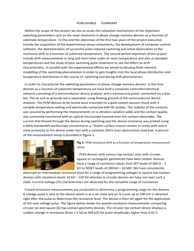
PUBLISHABLE SUMMARY Within the scope of this project we aim to study the relaxation mechanisms of the important switching parameters such as the reset resistance in phase change memory devices as a function of substrate temperature. To this end the objectives of the first two years of the project execution include the acquisition of the experimental setup components, the development of computer control software, the demonstration of successful pulse induced switching and initial observation of the resistance drift as a function of substrate temperature. The second period objectives of the project include drift measurements in long and short time scales at room temperature and also at elevated temperatures and the study of post switching pulse treatment to see the effect on drift characteristics. In parallel with the experimental efforts we aimed to develop finite element modelling of the switching phenomenon in order to gain insights into the local phase distribution and temperature distribution in the course of switching and during drift phenomenon. In order to characterize the switching parameters of phase change memory devices in the time domain as a function of substrate temperature we have built a computer controlled electrical network consisting of a semiconductor device analyzer and a nanosecond pulser connected via a bias tee. The dc and ac grounds were separated using floating ground of the semiconductor device analyzer. The PCM devices to be tested were mounted on a gold-coated vacuum chuck with a variable temperature setting and electrically contacted with RF probes. The stability of the contacts was assured by performing the measurements on a vibration isolation table and the contact quality was constantly monitored with an optical microscope zoomed onto the contact electrodes. The current that flowed through the device during switching and the device resistance was probed using a 6GHz bandwidth oscilloscope connected to a ~1kohm surface mount resistor in series with and in close proximity to the device under test with a constant 20mV (non-destructive) read bias. A picture of the measurement setup is provided in figure 1. Fig 1. PCM resistance drift as a function of temperature measurement setup. PCM devices with various top contact sizes with circular, square or rectangular geometries have been tested. Devices have a range of resistance values from SET levels of 200 Ω – 5 kΩ to RESET levels of 200 kΩ – 10 MΩ. We have consistently observed an intermediate resistance level for a range of programming voltages in square top-contact devices with resistance levels 10 kΩ – 120 kΩ whereas in circular devices we have not seen such a state. Current-Voltage (IV) characteristics are observed for the complete range of resistances. Pulsed-resistance measurements are conducted to determine a programming range for the devices. A voltage pulse is sent to the device which is at a set state and an IV curve up to 100 mV is obtained right after the pulse to determine the resistance level. The device is then set again for the application of the next voltage pulse. The figure below shows the pulsed-resistance measurements comparing circular (a) and square (b) top-contact geometry devices. The circular top contact device displays a sudden change in resistance (from 1.5 kΩ to 900 kΩ) for pulse amplitudes higher than 0.65 V. Fig 2. Pulsed-Resistance measurements for (a) 75 nm circular top contact device, (b) 90 nm square top contact device. Such a behavior is representative of circular top contact devices of 60-75 nm diameters that have a range of resistance values from 1 – 8 kΩ for set state and 800 kΩ – 3 MΩ for reset state. We consistently observe a multi-level switching for increasing voltage pulse amplitudes for square as well as rectangular top contact PCM cells. The example shown in Figure 2b is representative of a 90 nm square top contact device which displays a resistance increase from a set state of 700 Ω to a 24 kΩ resistance state, an intermediate resistance state, around 1.2 V and a second switching is observed around 1.45 V to a reset state with a resistance of 197 kΩ. It is clear that the 24 kΩ resistance state is a stable intermediate resistance state since there is a range of programming voltages between 1.25-1.4 V. Fig 3. Resistance drift data for set (blue diamonds), middle (black circles) and reset (red triangles) To elaborate the stability of the three resistance states: reset, set or middle state; we have monitored the time evolution of the resistance of the device under test after a switching operation. We have developed several Labview programming virtual instruments called VIs to perform different types of drift measurements such as drift under constant DC bias with a sourcemeter, or under constant DC bias with a battery, drift after discrete time intervals (like 5 minutes) recorded as IV curves for long periods of time (up to a day). Fig 4. Resistance drift coefficient of the intermadiate state as a function of temperature. The temperature dependent studies of the drift behaviour showed that the drift is accelerated at higher temperatures consistent with structural relaxation model. This also indicates that using those phase change materials with glass transition temperatures above that of GST may help improve the stability of the resistance levels. The detailed characterization of the drift characteristics we have obtained in this project allowed us to identify the source of the drift to be mainly structural relaxation. The different device geometries led to the stabilization of different resistance states during programming. We have shown that an intermediate resistance state rather than a RESET state may be preferrable for better device performance in terms of long term reliability. Our study will lead to optimum device designs with better stability in time with the use of intermediate resistance states rather than the reset state in future PCM devices. Therefore commercialization of more reliable and stable pcm devices will be possible for future data storage applications. Contact: Assoc. Prof. Ozhan Ozatay for more details. Email: ozhan.ozatay@boun.edu.tr


