ix. low power synthesis
advertisement

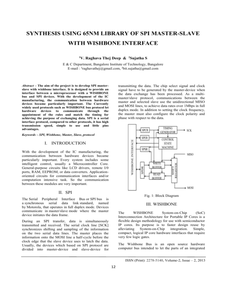
SYNTHESIS USING 65NM LIBRARY OF SPI MASTER-SLAVE WITH WISHBONE INTERFACE 1 V. Raghava Thej Deep & 2Sujatha S E & C Department, Bangalore Institute of Technology, Bangalore E-mail : 1raghavathej@gmail.com, 2bit.sujatha@gmail.com Abstract – The aim of the project is to develop SPI masterslave with wishbone interface. It is designed to provide an interface between a microprocessor with a WISHBONE bus and SPI devices. With the development of the IC manufacturing, the communication between hardware devices became particularly important. The Currently widely used protocols such as WISHBONE bus protocol let hardware devices to communicate through the appointment of the rules and match the timing for achieving the purpose of exchanging data. SPI is a serial interface protocol, compared to other protocols, it has high transmission speed, simple to use and little pins advantages. transmitting the data. The chip select signal and clock signal have to be generated by the master-device when the data exchange has been processed. As a multimaster/slave protocol, communications between the master and selected slave use the unidirectional MISO and MOSI lines, to achieve data rates over 1Mbps in full duplex mode. In addition to setting the clock frequency, the master must also configure the clock polarity and phase with respect to the data. Keywords – SPI, Wishbone, Master, Slave, protocol I. INTRODUCTION With the development of the IC manufacturing, the communication between hardware devices became particularly important. Every system includes some intelligent control, usually a Microcontroller Core. General-purpose circuits like LCD drivers, remote I/0 ports, RAM, EEPROM, or data converters. Applicationoriented circuits for communication interfaces and/or computation intensive task. So the communication between these modules are very important. II. SPI Fig. 1: Block Diagram The Serial Peripheral Interface Bus or SPI bus is a synchronous serial data link standard, named by Motorola, that operates in full duplex mode. Devices communicate in master/slave mode where the master device initiates the data frame. III. WISHBONE The WISHBONE System-on-Chip (SoC) Interconnection Architecture for Portable IP Cores is a flexible design methodology for use with semiconductor IP cores. Its purpose is to faster design reuse by alleviating System-on-Chip integration. Simple, compact, logical IP core hardware interfaces that require very few logic gates. During an SPI transfer, data is simultaneously transmitted and received. The serial clock line [SCK] synchronizes shifting and sampling of the information on the two serial data lines. The master places the information onto the MOSI line a half-cycle before the clock edge that the slave device uses to latch the data. Usually, the devices which based on SPI protocol are divided into master-device and slave-device for The Wishbone Bus is an open source hardware computer bus intended to let the parts of an integrated ISSN (Print): 2278-5140, Volume-2, Issue – 2, 2013 12 International Journal of Advanced Computer Engineering and Communication Technology (IJACECT) circuit communicate with each other. The aim is to allow the connection of differing cores to each other inside of a chip. WISHBONE uses MASTER/SLAVE architecture. That means that functional modules with MASTER interfaces initiate data transactions to participating SLAVE interfaces. Here all internal WISHBONE logic is registered to the rising edge of the [clk_i] clock input. So, master clock decides the data to send or not. The active low asynchronous reset input [rst_i] forces the core to restart. All internal registers are preset and all statemachines are set to an initial state. The interrupt request output is asserted when the core needs service from the host system. When asserted, the cycle input [cyc_i] indicates that a valid bus cycle is in progress. The logical AND function of [cyc_i] and [stb_i] indicates a valid transfer cycle to/from the core. So when only the cycle input is high strobe signal is high. The strobe input [stb_i] is asserted when the core is being addressed. The core only responds to WISHBONE cycles when [stb_i] is asserted, except for the [rst_i], which always receive a response. Fig. 2: Verification Methodology Flow V. SIMULATION The address array input [adr_i] is used to pass a binary coded address to the core. The most significant bit is at the higher number of the array. When asserted, the write enable input [we_i] indicates that the current bus cycle is a write cycle. When negated, it indicates that the current bus cycle is a read cycle. The data array input [dat_i] is used to pass binary data from the current WISHBONE Master to the core. All data transfers are 8 bit wide. The data array output [dat_o] is used to pass binary data from the core to the current WISHBONE Master. All data transfers are 8 bit wide. When asserted, the acknowledge output [ack_o] indicates the normal termination of a valid bus cycle. The use of a CAD tool that mimics the behavior of the actual circuit through a collection of sub-circuit models enabling designers to test and verify the design. IV. VERIFICATION METHODOLOGY The Design is coded in Verilog, RTL Code is compiled to check semantic and syntactical errors. With test bench coded in Verilog, RTL code is simulated and waveform is observed. After simulation, code coverage is carried out to increase the confidence of code. Various coverages are observed such as Branch, Toggle and Expression. Synthesis is carried out to generate technology specific Gate-level Netlist. Different Low Power constraints are added for Low power synthesis. The figure 2 shows Verification methodology of the project. Fig. 3: Schematic Tracer Result Schematic tracer shown in Figure 3 shows the overview of the design and various stimulus that is applied from the test bench. ISSN (Print): 2278-5140, Volume-2, Issue – 2, 2013 13 International Journal of Advanced Computer Engineering and Communication Technology (IJACECT) VII. SYNTHESIS Synthesis is the translation process from a description of a hardware device at higher abstraction level into an optimized implementation on a lower level abstraction and generation of technology specified Gate level Netlist. A 65nm model library used for synthesis. Fig. 4: Waveform Waveform as shown in figure 4 depicts if the functionality of the design is observed correctly. Fig. 6: Synthesis Result VI. CODE COVERAGE VIII. SOURCES OF POWER DISSIPATION Source of Power dissipation in CMOS are- A set of metrics at the behavioral or RTL abstraction level which define the extent to which the design has been exercised. Toggle coverage reports the number of times each bit of a register or wire has toggled its value. block coverage‚ defines a sequence of statements with no branches to be a block. Condition coverage or expression coverage records the number of times each permutation of the terms of a Boolean expression cause the complete expression to evaluate to true or false. A. Static dissipation 1. Sub threshold conduction when the transistors are off. Both NMOS and PMOS transistors have a gate–source threshold voltage, below which the current (called sub threshold current) through the device drops exponentially 2. Leakage current through reverse biased diodes. Small reverse leakage currents are formed due to formation of reverse bias between diffusion regions and wells (for e.g., p-type diffusion vs. n-well), wells and substrate (for e.g., n-well vs. p-substrate). B. Dynamic Dissipation 1. Charging and discharging of load capacitances. CMOS circuits dissipate power by charging the various load capacitances (mostly gate and wire capacitance, but also drain and some source capacitances) whenever they are switched. In one complete cycle of CMOS logic, current flows from VDD to the load capacitance to charge it and then flows from the charged load capacitance to ground during discharge. 2. Short circuit power dissipation Since there is a finite rise/fall time for both pMOS and nMOS, during transition from on/off to off/on, both the transistors will be on for a small period of Fig. 5: Overall Code Coverage ISSN (Print): 2278-5140, Volume-2, Issue – 2, 2013 14 International Journal of Advanced Computer Engineering and Communication Technology (IJACECT) time in which current will find a path directly from VDD to ground, hence creating a short circuit current. Dynamic Power is reduced with different low power techniques as shown in Figure 7. IX. LOW POWER SYNTHESIS The different low power option used during low power synthesis areA. Multi Vt. Multiple threshold voltage techniques use hvt, nvt and lvt. Selection of either of the libraries reduces the dynamic power. Each technology specific library will have different power dissipation for each component/gates. Thus, selecting an appropriate library is necessary. B. Avoid Cells that consume more power. For a given technology specific libraries a single design/operation can be mapped by using various gates of the same library. A single library possesses different gates which perform same operation but, the characteristics (power, timing, area, capacitance, resistance) of those gates are different. So, avoiding of more power consuming cells are important. Fig. 7: Dynamic power for different libraries Table 1: Dynamic Power in nW. Dynamic Power HVT NVT LVT C. Clock Gating Clock gating is a popular technique used in many synchronous circuits for reducing dynamic power dissipation. Clock gating saves power by adding more logic to a circuit to prune the clock tree. Pruning the clock disables portions of the circuitry so that the flipflops in them do not have to switch states. Switching states consumes power. When not being switched, the switching power consumption goes to zero, and only leakage currents are incurred. Synthesis Avoid Cells Clock Gating 213399.273 206549.661 150790.773 208693.114 208690.221 152604.123 217119.636 213558.875 154506.153 Statistics shown in figure 8 shows that area increases after avoiding cells that consume more power, but gets educed after clock gating. Area count gradually reduced across the libraries shown in order. The primary aim of low power synthesis is to minimize total power of the design or reducing the dynamic power with negligible compromise in leakage power and area, without timing violation. The various low power techniques used are insertion of clock gating, choosing different Vth libraries and avoiding cells which consume more power. X. RESULTS The design is coded using Verilog HDL and Simulated to observe the behavior. RTL Design is synthesized by applying library, design and timing constraints using 65nm library. Different Low power options are added and various reports such as Dynamic and leakage power, area and Timing are tabulated. The synthesis results are compared with low power synthesis. Fig. 8: Area report for different libraries ISSN (Print): 2278-5140, Volume-2, Issue – 2, 2013 15 International Journal of Advanced Computer Engineering and Communication Technology (IJACECT) [5] Specification for the: “WISHBONE System-onChip (SoC) Interconnection Architecture for Portable IP Cores ”Revision: B.3, Released: September 7, 2002. [6] Archana Ramesh R and M.S.R.Sekhar “Design and Verification of Serial Peripheral Interface using OVM” International Journal of Electronics Communication and Computer Technology (IJECCT) Volume 2 Issue 6. [7] Baowen Zhou, Dong Li and Gang Lu “Design of high-speed and reusable SPI IP core based on Wishbone interface” Electrical and Control Engineering (ICECE), 2011 International Conference. [8] Mohandeep Sharma and Dilip Kumar “WISHBONE bus architecture – a survey and comparison” International Journal of VLSI design & Communication Systems (VLSICS) Vol.3, No.2, April 2012. [9] Run Chen, Shi-zhen Huang, Wei Lin, Lei Li, "Design and Implementation of a Reused Interface," icise, pp.2603-2605, 2009 First International Conference. [10] Changlei Dongye “Design of the on-chip bus based on Wishbone” Electronics, Communications and Control (ICECC), 2011 International Conference. [11] Sharma. M and Kumar D “Design and synthesis of Wishbone bus Dataflow interface architecture for SoC integration” India Conference (INDICON), 2012 Annual IEEE. [12] Ayas Kanta Swain and Kamala Kanta Mahapatra “Design and Verification of Wishbone Bus Interface for System-on-Chip Integration” 2010 Annual IEEE India Conference (INDICON). Gao Yong, Yang Yuan and Fan Bei ”The application of bus coding in designing of low power SoC based on Wishbone” Computer Science and Information Processing (CSIP), 2012 International Conference. [13] K.Aditya, M. Sivakumar, Fazal Noorbasha and T. Praveen Blessington “Design and Functional Verification of A SPI Master Slave Core Using System Verilog” International Journal of Soft Computing and Engineering (IJSCE) ISSN: 2231-2307, Volume-2, Issue-2, May 2012. Jianlong Zhang, Chunyu Wu, Wenjing Zhang and Jiwei Wang “The design and realization of a comprehensive SPI interface controller” Mechanic Automation and Control Engineering (MACE), 2011 Second International Conference. [14] Zhili Zhou, Zheng Xie, Xin'an Wang and Teng Wang “Development of verification environment for SPI master interface using SystemVerilog” Signal Processing (ICSP), 2012 IEEE 11th International Conference. [15] Tianxiang Liu and Yunfeng Wang “IP design of universal multiple devices SPI interface” (ASID), 2011 IEEE International Conference. Table 2: Area in umeter2 Area in um2 Synthesis Avoid Cells Clock Gating HVT 1151 1162 1108 NVT 1148 1176 1111 LVT 1148 1192 1119 Cell count decreases after various low power options as shown in figure 9. Also, count reduces comparing from different libraries – lvt, nvt and hvt. Fig. 9: No. of Cells utilized for various libraries. Table 3: Cell count for different libraries No. of Cells Synthesis Avoid Cells Clock Gating HVT 242 243 249 NVT 235 247 252 LVT 235 260 266 XI. REFERENCES [1] [2] [3] www.opencore.org.Simon Srot. “SPI Master Core Specification”, Rev.0.6. May 16, 2007. [4] “Design and Implementation of a Reused Interface” 978-0-7695-3887-7/09/$26.00 ©2009 IEEE. ISSN (Print): 2278-5140, Volume-2, Issue – 2, 2013 16


