Palesko_Amy_1
advertisement
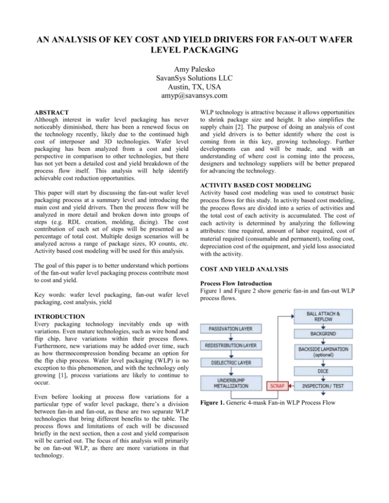
AN ANALYSIS OF KEY COST AND YIELD DRIVERS FOR FAN-OUT WAFER LEVEL PACKAGING Amy Palesko SavanSys Solutions LLC Austin, TX, USA amyp@savansys.com ABSTRACT Although interest in wafer level packaging has never noticeably diminished, there has been a renewed focus on the technology recently, likely due to the continued high cost of interposer and 3D technologies. Wafer level packaging has been analyzed from a cost and yield perspective in comparison to other technologies, but there has not yet been a detailed cost and yield breakdown of the process flow itself. This analysis will help identify achievable cost reduction opportunities. WLP technology is attractive because it allows opportunities to shrink package size and height. It also simplifies the supply chain [2]. The purpose of doing an analysis of cost and yield drivers is to better identify where the cost is coming from in this key, growing technology. Further developments can and will be made, and with an understanding of where cost is coming into the process, designers and technology suppliers will be better prepared for advancing the technology. This paper will start by discussing the fan-out wafer level packaging process at a summary level and introducing the main cost and yield drivers. Then the process flow will be analyzed in more detail and broken down into groups of steps (e.g. RDL creation, molding, dicing). The cost contribution of each set of steps will be presented as a percentage of total cost. Multiple design scenarios will be analyzed across a range of package sizes, IO counts, etc. Activity based cost modeling will be used for this analysis. ACTIVITY BASED COST MODELING Activity based cost modeling was used to construct basic process flows for this study. In activity based cost modeling, the process flows are divided into a series of activities and the total cost of each activity is accumulated. The cost of each activity is determined by analyzing the following attributes: time required, amount of labor required, cost of material required (consumable and permanent), tooling cost, depreciation cost of the equipment, and yield loss associated with the activity. The goal of this paper is to better understand which portions of the fan-out wafer level packaging process contribute most to cost and yield. Key words: wafer level packaging, fan-out wafer level packaging, cost analysis, yield COST AND YIELD ANALYSIS Process Flow Introduction Figure 1 and Figure 2 show generic fan-in and fan-out WLP process flows. INTRODUCTION Every packaging technology inevitably ends up with variations. Even mature technologies, such as wire bond and flip chip, have variations within their process flows. Furthermore, new variations may be added over time, such as how thermocompression bonding became an option for the flip chip process. Wafer level packaging (WLP) is no exception to this phenomenon, and with the technology only growing [1], process variations are likely to continue to occur. Even before looking at process flow variations for a particular type of wafer level package, there’s a division between fan-in and fan-out, as these are two separate WLP technologies that bring different benefits to the table. The process flows and limitations of each will be discussed briefly in the next section, then a cost and yield comparison will be carried out. The focus of this analysis will primarily be on fan-out WLP, as there are more variations in that technology. Figure 1. Generic 4-mask Fan-in WLP Process Flow so the generic fan-in and fan-out processes shown in Figures 1 and 2 are the basis for all of the cost breakdowns. Fan-in WLP versus Fan-out WLP Comparing fan-in to fan-out WLP is similar to comparing apples to oranges—it’s not a fair comparison in that these technologies will often serve different designs and purposes. They contain some of the same series of steps, but not all— the fan-out process is longer and more complicated. Nevertheless, these two options will be compared side-byside for a few purposes. The first goal is to understand the ways in which the cost drivers differ between the flows, and the second purpose is to consider the yield implications. Figure 2. Generic Fan-out WLP Process Flow Fan-in WLP involves forming the package on the die before the wafer is diced. This results in a package that is the same size as the die. The fan-in process can be seen as similar to the bumping process for flip chip packages [3]. The process flow in Figure 1 is the process flow for a 4-mask RDL and bump structure (there are other options for fan-in, like 2 and 3 mask as well). This 4-mask process results in an metal RDL layer between two dielectric layers, as well as including underbump metallization [4], [5]. In addition to the options for the fan-in process flow (e.g. number of masks), there are variations on the fan-out WLP process as well. Infineon has eWLB (embedded wafer level BGA), which is licensed to multiple companies; TSMC has InFO and Freescale has RCP (redistributed chip package), neither of which has reached HVM [6]. Those are just a few examples. While these versions of fan-out WLP are all different from each other, they share many of the same characteristics of the generic process flow. For example, one main difference between the RCP flow and other options is the existence of an embedded ground plane (EGP) early in the process— mounting tape is placed on a substrate and then, before the die are placed on the adhesive as they would be in the typical process, an embedded ground plane is placed before the die. The die are placed into openings in the EGP. So this is an extra step that would add some material and processes costs, but may save cost in the long run as it provides improvement in reliability [7]. Minor differences between different types of fan-in and fanout WLP will not be analyzed in detail in this paper. The main cost contributors in the WLP processes will not change appreciably even with small changes to the process, Table 1. Fan-in versus fan-out design parameters Fan-in Fan-out 6x6mm Die size 6x6mm 10x10mm Package Size 200 529 # of I/Os 0.4mm Pitch All costs will presented at as a percentage of total cost. Only direct costs are included in these calculations—overhead, profit margin, and other indirect costs have been left out to better analyze the cost contributors to the process flow itself. The cost of the incoming die, which would usually be seen as a material cost with our cost modeling methods, is also not included. It should also be noted that all cost analyses were run using Taiwan labor rates. The two graphs in Figure 3 break the flows down into process sections. The fan-in chart has fewer categories since the process flow is shorter, and the portions of the process flow all contribute a similar amount of cost. If the process flow was broken down in a different way, the graph wouldn’t have such even segments. For example, the two dielectric layers (called polyimide and passivation in these categories), underbump metallization, and redistribution layer (RDL) steps are all similar in that they are preparing the layers of connection between the bump and the substrate. If grouped together under the umbrella of interconnect formation, those four portions of the flow represent half of the total cost. The fan-out WLP pie chart has more components due to the complexity of the process. The largest contributor to the cost here is the RDL process. At first glance, it may seem strange that both process flows have a set of RDL steps, but those steps are a much higher percentage of cost for the longer and more expensive flow. This highlights one of the key differences between these technologies. The cost of the RDL is tied to the package size. The package size is limited by die size in fan-in packaging, but it is the opposite case for a fan-out package. The RDL is used to spread (or fan) out the connections (and thus to allow for more connections). Therefore, the RDL cost is much higher in the fan-out case because it is a 10x10mm package. There are more material and processing costs associated with those steps. The second way to compare fan-in to fan-out is to look at the types of cost contributing to each, where “types of cost” refers to the most basic levels of cost: labor, material, and so on. Figure 3. Percent of Cost by Process Flow Section, Fan-in vs. Fan-out Backgrinding and backside lamination are about the same percentage of total cost for both process flows, despite the different number of steps and overall different costs. This occurs because the activities are driven by surface area, so although the cost on an absolute level increases in this category for the fan-out process, the other costs also increased, resulting in it being a similar percentage of the total cost. It should also be noted that backside lamination is an optional process, but it was included in all of the analyses to maintain a process flow baseline and to understand the impact of its addition. There are three cost contributors that are missing completely from the fan-in process: the bonding of the die, the subsequent compression molding, and the steps that involve debonding the molded die from the carrier wafer. By looking at these pie charts, it’s not only easy to see which parts of the process are unique to fan-out WLP, but also to determine which portions of each process flow are major cost adders. Figure 4. Breakdown by Cost Category, Fan-in vs. Fan-out Despite the differences in the process flows at the technology level, the contributions from the different types of cost are fairly equal for both options. Capital is a huge cost driver, which is unsurprising, as this tends to be a factor in any semiconductor process. The second highest cost contributor in both process flows is material. For fan-out WLP, the highest material contributor is the mold compound, and the rest of the material costs come largely from the dielectric, backside lamination, and flux and ball attach. The material contributors in the fan-in process are the dielectric materials, the backside lamination, and the flux and ball attach as well. One key difference between the flows is the portion of cost from yield. While a difference of 4% is not huge, it’s not inconsequential. Why does the shorter, less complicated fanin process have a higher yield hit than the longer and more complex fan-out process flow? As stated before, this is not an apples to apples comparison, and that holds true for yield as well. In the fan-out process, there are two times when scrapping of bad die may occur. When the wafers come in and are prepared and diced, there is an opportunity to scrap the bad die before proceeding with placing them on the tape for the package to be formed around them. As the process flow proceeds, certain steps have an impact on yield, such as RDL creation and ball attach. Once the fully formed packages are diced, there is another opportunity for scrap. On the other hand, in the fan-in process, the only scrap opportunity occurs at the end. So, where bad die were scrapped in the fan-out process and prevented from being carried into the flow and having expensive processing done on them, in the fan-in process, bad die come in, go through expensive processing, and only then are scrapped. The key takeaway from this section is that, although there are different drivers from a design perspective leading toward either fan-in or fan-out selection, one of the key factors when using fan-in technology is yield. A high quality incoming wafer should be a priority. The rest of this paper will focus on fan-out wafer level packaging examples. Conclusions that can be applied to real-life technology scenarios will be drawn in each section. Analysis of a Two-die Fan-out Wafer Level Package In this section, a more complicated fan-out WLP design is analyzed for cost breakdown. While larger package sizes are certainly being developed, 14x14mm is one of the largest eWLB type fan-out packages in production right now [8], and that is the package size selected for this evaluation. Table 2. Two-die fan-out package design parameters Fan-out Package 2 die, each at 6x6mm Die size 14x14mm Package Size 2 # of RDLs 1000 # of I/Os As before, this is an examination of direct costs associated with the fan-out WLP process. The cost of the incoming die is not included in these (or any following) results, and overhead and profit margin are likewise not included. Figure 5. Percent of Cost by Process Flow Section, Two-die Example A number of factors are apparent when this graph is compared to that of the single die fan-out WLP in the first comparison. Now that there are two RDLs instead of only one, the percentage of cost in this two-die example is 59%, instead of the 40% it was for the single die example. This isn’t just driven by the fact that there are two RDLs, but also because the package size is larger. Within the RDL category, the majority of cost is capital, associated with the expensive equipment required for this process. If the capital costs in the RDL process were cut in half, this category would drop from 59% of the total process flow cost down to 51%. The takeaway here is that any process improvement that can be done to either reduce the cost of the equipment required for RDL creation or reduce the amount of time required on the tool may have a significant impact on the cost competitiveness of a fan-out WLP process. All other cost contributors in the process flow are a similar percentage to what they were in the single die scenario, each reduced slightly due to the increased RDL percentage, which means that most cost contributors in the fan-out WLP process scale with package size. A comparison of the types of cost for this two-die design is included in Figure 6. Compared to the single die example, the percentage of cost from both material and capital has gone done. This is because there is a higher percentage of cost now from yield hit. The yield impact has tripled rather than doubled because the effect of yield is cumulative. The RDL process is responsible for the majority of the yield impact in the fan-out process, and there are two RDLs rather than just one in this example, creating a compounding effect. Figure 6. Breakdown by Cost Category, Two-die Example Smaller versus Larger Package Size The goal of this next comparison is to examine the trade-off between package size and density, or the number of RDLs. This is a situation in which the same size die is placed in two different packages—one smaller and therefore requiring more routing layers to distribute the I/Os, and one larger with less dense routing. The I/O count is kept static between the two examples here to limit the changing variables and focus on RDL count and package size; it should be noted that in a real-life scenario, the reason for going to a larger package size would generally be to have more I/Os. Table 3. Smaller vs. larger package design parameters Smaller Package Larger Package 6x6mm 6x6mm Die size 7x7mm 9x9mm Package Size 2 1 # of RDLs 470 470 # of I/Os The cost contributions by process flow breakdown are shown in Figure 7. Three of the cost contributors—back grinding and lamination, mold, and debonding from the carrier wafer—scale with the package size. On the other hand, the cost associated with RDLs appears to scale with the number of RDLs, but this is not strictly the case. In these graphs, while the RDL cost appears to be much higher when there are two RDLs, the absolute cost difference between RDL processing costs is only 2.4 cents per package. In other words, the total cost of the RDL processing that goes into the smaller package that utilizes two RDLs is only 2.4 cents more expensive than the RDL processing that goes into the larger package with the single RDL. The reason the percentage contribution from RDL processing looks so much smaller in the single RDL scenario is because the other contributors have scaled so much with the package size. Figure 7. Percent of Cost by Process Flow Section, Smaller vs. Larger Package The major takeaway from this comparison is that, although RDL processing is one of the most expensive parts of the fan-out WLP process, package size is also a notable cost driver. In terms of absolute cost, in this example the smaller, more dense package was actually more cost-effective. The next set of graphs in Figure 8 are almost identical. When comparing these two designs from the perspective of types of cost, all of the values are very close. The impact of capital cost has been covered in previous sections, and this new analysis doesn’t alter that conclusion. While the contribution of material is not nearly as high as that of equipment, it’s not a negligible factor. For those seeking to make the fan-out WLP process more cost friendly, advancement in the materials used would make a considerable difference. For example, in the scenario above with one die and two RDLs in a small package, if the material contributions in the RDL steps were cut by one third, the percentage contribution toward the total would shift by a full 2%. This is not insignificant. A tangible example of this would be if the price of photoimagable dielectrics dropped, it would have a direct impact on the total cost of the process. technologies share a similar breakdown in terms of the types of cost, with capital being the highest percentage of cost and material the second. The fan-in process, despite being simpler, had a higher percentage of cost due to yield hit. This is because there is only one opportunities to scrap bad die in the fan-in flow, while there are two opportunities in the fan-out flow. The key drivers of fan-out WLP cost were shown to be related to package size. It was also shown that, across all designs analyzed in this paper, the RDL creation steps are the largest cost contributors in the process flow. Any improvements that can be made in the capital or material factors for RDL creation would have an impact on the overall process. REFERENCES [1] P Singer, “Fan-out wafer level packaging set to expand”, http://electroiq.com/, 2015. [2] STATS ChipPAC, “Next Generation eWLB (embedded Wafer Level BGA) Packaging”, EPTC, 2010. [3] X. Fan, “Wafer Level Packaging (WLP): Fan-in-, Fanout and Three-dimensional Integration”, Int. Conf. on Thermal, Mechanical and Multiphysics Simulation and Experiments in Micro-Electronics and Micro-System , 2010. [4] EP & Dee website, “Wafer Level Chip Scale Package (WLCSP), http://www.epd-ee.eu/article/9008, 2015. [5] Amkor Technology website, “Wafer Level Packaging” section. [6] P. Garrou, “Insights from Leading Edge,” Solid State Technology website, April 2015. [7] Freescale Semiconductor Inc., “Implementation of a Mobile Phone Module with Redistributed Chip Packaging”, ECTC, 2008. Figure 8. Breakdown by Cost Category, Smaller vs. Larger Package Example CONCLUSION This paper analyzed the wafer level packaging processes from the perspective of cost contributions as percentages of total direct cost. Both fan-in and fan-out processes were analyzed by looking at portions of the process flow, and by looking at types of cost. The goal was to analyze where the cost is coming from and how the cost contributors shift with different designs. With a greater understanding of these cost drivers, material and equipment suppliers can understand which process advantages have a measureable impact on the total process flow. Fan-in WLP was shown to be the simpler process flow of the two. Despite the process flow differences, both [8] STATS ChipPAC website, “eWLB (FOWLP Technology)” section.

