The Technology
advertisement
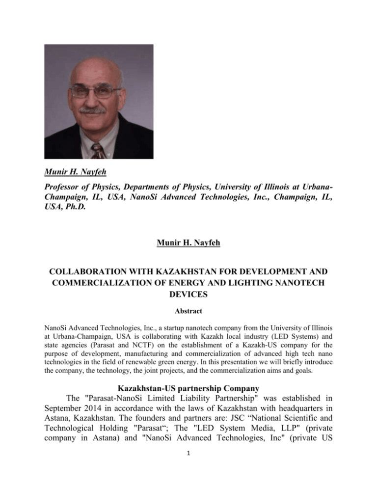
Munir H. Nayfeh Professor of Physics, Departments of Physics, University of Illinois at UrbanaChampaign, IL, USA, NanoSi Advanced Technologies, Inc., Champaign, IL, USA, Ph.D. Munir H. Nayfeh COLLABORATION WITH KAZAKHSTAN FOR DEVELOPMENT AND COMMERCIALIZATION OF ENERGY AND LIGHTING NANOTECH DEVICES Abstract NanoSi Advanced Technologies, Inc., a startup nanotech company from the University of Illinois at Urbana-Champaign, USA is collaborating with Kazakh local industry (LED Systems) and state agencies (Parasat and NCTF) on the establishment of a Kazakh-US company for the purpose of development, manufacturing and commercialization of advanced high tech nano technologies in the field of renewable green energy. In this presentation we will briefly introduce the company, the technology, the joint projects, and the commercialization aims and goals. Kazakhstan-US partnership Company The "Parasat-NanoSi Limited Liability Partnership" was established in September 2014 in accordance with the laws of Kazakhstan with headquarters in Astana, Kazakhstan. The founders and partners are: JSC “National Scientific and Technological Holding "Parasat“; The "LED System Media, LLP" (private company in Astana) and "NanoSi Advanced Technologies, Inc" (private US 1 company in Champaign, USA, with the National Center for Technology Foresight (NCTF), Astana being none-voting advisor. The goal of the Partnership includes production of nanotechnology-based industrial products; development of applied researches; innovations in nanotechnology; and applications. The company may have international activities; the partnership may set up non-legal branches (representative offices) as well as carry out foreign economic activity. The company will follow an “open innovation” business model The Technology Breakthrough research led by the US partner and associated institutions to inventing nano-engineered, discreetly-sized silicon nanoparticles that are nonnaturally occurring form of elemental silicon. They provide enabling optical, electronic and bio applications. Unlike bulk, they are spectacularly luminescent (“glow”) under UV-illumination with specific size-dependent color (red-greenblue), with single-ones being detectable. The silicon nano particle material is introduced to answer the challenge of getting disparate materials to work together (integrate), especially in electronics and photonics. Silicon nanoparticles alleviate this problem as silicon-to-silicon products are easier to engineer. Thus the technology can be integrated in the silicon industry. Moreover there is a need for a universal-wide-platform nanomaterial that provides diverse applications, while being amenable to mass-production and commercialization. As to freedom of operation, the technology is protected by 22 US-European patents (16 issued), and it is considered a green technology, that is it is least toxic, most biocompatible for consumer application From the scientific point of view, the achievements are at the frontiers of science and technology and knowledge, with 60 refereed-articles published, and wide-reporting in magazines, encyclopedias, and dailies, including Nature, Physics Today, Physics World, Britannica, McGraw Hill, World Book, New Scientist, American Scientist, Business2.0, Washington Post, which earned us “nanotech pioneer” status by Wiley. With regard to business, the technology attracted global collaborations with academia and industry as well as industrial and government funding including US (PolyBrite, US-Army), Japan (Sharp, Panasonic), Vietnam (SHTP), Saudi Arabia (ARAMCO, KACST), Kazakhstan (Parasat), Korea (Samsung), Taiwan (Wintek), Canada (Sungen-Octillion). On the academia side, collaborations with Saratov State University, MIT, Cleveland State, Wales University, Hawaii University, King Fahd University, King Saud University, University of Jordan, Masdar Institute of S and T, etc.. Government and foundation funding came from the US National Science Foundation, State of Illinois, US Army, and Grainger Foundation. 2 We and colleagues at the University of Illinois and NanoSi Advanced Technologies, Inc developed a number of advanced nano-device prototypes, including fuel cells, flash memory, solar cell, super capacitor, glucose sensor, enhanced oil recovery material, nanophosphor, photdetector, which are being promoted by the US partner and the US-Kazakhstan company. A consortium of US scientists engaged OIC to develop nano-based low-cost devices, useful in remote-poor areas, and to establish an international nanotechnology center. Technology commercialization features The procedure of manufacturing of the silicon nanomaterial which was initially developed by the partnering US Company “NanoSi” offer very advantageous features for commercialization. Those include High quality (uniform, bright, stable particles): come in four uniform sizes or identical sizes, which allows reconstitutions in high-quality solids and films for subsequent use in light mixing Easy to manufacture: uses common raw materials and chemicals; Silicon, the most abundant, cheapest and least toxic semiconductor material; Acids and hydrogen peroxide; Low power electricity; Table-top setups; Room temperature reaction temperature Patent protected; 22 US patents (16 issued) as well a number of foreign patents. Amenable to mass production: The process is very efficient, scalable and can be automated; Quick process (30-45 minutes to completion) Easy to use: Differently sized silicon nanoprticles can be excited with a single source to obtain various colors, making them easier to use The technology has proven to be a silicon platform technology with diverse applications that include: electronics (flash nano memory); photonics (micro lasers, UV photodetectors); energy harvest & lighting (solar cells, Nano phosphor LED, supercapacitors, catalyst, fuel cells); substance sensors (glucose and Dopamine); biomedical fluorescent tags; cosmetics, skincare, and hair care; nano high tech paint: monitoring & protecting the health of large military and civil structures. Priority Projects in Kazakhstan The projects on developments have been defined as the first projects to be implemented by the Partnership. Those include: • Factory for production of nanosilicon for company use, and domestic and international sale. • White Nano Phosphorus for LED 3 • • • • NanoSi Super Capacitors for energy storage NanoSi fuel cells Hands-on-training programs & Education Development of IP in the nano domain Business Model Sell locally manufactured nano particle material, sell or lease production equipment, create partnerships (open innovation) for production of advanced devices Innovation in development and manufacturing Parasat-NanoSi will not sit idle. It will innovate, research and develop to stay ahead of present competition or future ones. For instance it will have concerted effort to: Refine Particle Production Develop new ways of making nano particles Identify new advanced applications Design and produce Prototype Venture in international markets and sales Generate IP and Trademarks Reach out to domestic and international investors Conclusion: Parasat-Nanosi is seeking partners and investment funds from private investment corporations, angel investors, industry, and state agencies. 4
