CNR-SPIN (UOS L`Aquila) Via Vetoio 10, 67100, L`Aquila, Italy
advertisement
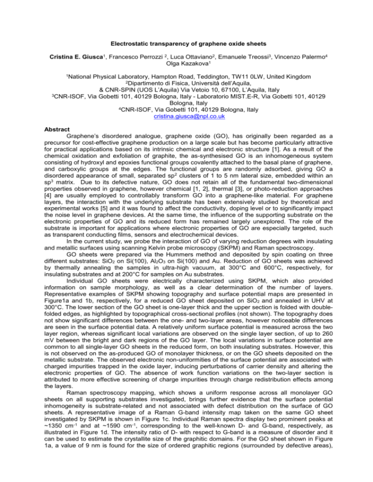
Electrostatic transparency of graphene oxide sheets Cristina E. Giusca1, Francesco Perrozzi 2, Luca Ottaviano2, Emanuele Treossi3, Vincenzo Palermo4 Olga Kazakova1 1National Physical Laboratory, Hampton Road, Teddington, TW11 0LW, United Kingdom 2Dipartimento di Fisica, Università dell’Aquila, & CNR-SPIN (UOS L’Aquila) Via Vetoio 10, 67100, L’Aquila, Italy 3CNR-ISOF, Via Gobetti 101, 40129 Bologna, Italy - Laboratorio MIST.E-R, Via Gobetti 101, 40129 Bologna, Italy 4CNR-ISOF, Via Gobetti 101, 40129 Bologna, Italy cristina.giusca@npl.co.uk Abstract Graphene’s disordered analogue, graphene oxide (GO), has originally been regarded as a precursor for cost-effective graphene production on a large scale but has become particularly attractive for practical applications based on its intrinsic chemical and electronic structure [1]. As a result of the chemical oxidation and exfoliation of graphite, the as-synthesised GO is an inhomogeneous system consisting of hydroxyl and epoxies functional groups covalently attached to the basal plane of graphene, and carboxylic groups at the edges. The functional groups are randomly adsorbed, giving GO a disordered appearance of small, separated sp 2 clusters of 1 to 5 nm lateral size, embedded within an sp3 matrix. Due to its defective nature, GO does not retain all of the fundamental two-dimensional properties observed in graphene, however chemical [1, 2], thermal [3], or photo-reduction approaches [4] are usually employed to controllably transform GO into a graphene-like material. For graphene layers, the interaction with the underlying substrate has been extensively studied by theoretical and experimental works [5] and it was found to affect the conductivity, doping level or to significantly impact the noise level in graphene devices. At the same time, the influence of the supporting substrate on the electronic properties of GO and its reduced form has remained largely unexplored. The role of the substrate is important for applications where electronic properties of GO are especially targeted, such as transparent conducting films, sensors and electrochemical devices. In the current study, we probe the interaction of GO of varying reduction degrees with insulating and metallic surfaces using scanning Kelvin probe microscopy (SKPM) and Raman spectroscopy. GO sheets were prepared via the Hummers method and deposited by spin coating on three different substrates: SiO2 on Si(100), Al2O3 on Si(100) and Au. Reduction of GO sheets was achieved by thermally annealing the samples in ultra-high vacuum, at 300°C and 600°C, respectively, for insulating substrates and at 200°C for samples on Au substrates. Individual GO sheets were electrically characterized using SKPM, which also provided information on sample morphology, as well as a clear determination of the number of layers. Representative examples of SKPM showing topography and surface potential maps are presented in Figure1a and 1b, respectively, for a reduced GO sheet deposited on SiO2 and annealed in UHV at 300°C. The lower section of the GO sheet is one-layer thick and the upper section is folded with doublefolded edges, as highlighted by topographical cross-sectional profiles (not shown). The topography does not show significant differences between the one- and two-layer areas, however noticeable differences are seen in the surface potential data. A relatively uniform surface potential is measured across the two layer region, whereas significant local variations are observed on the single layer section, of up to 260 mV between the bright and dark regions of the GO layer. The local variations in surface potential are common to all single-layer GO sheets in the reduced form, on both insulating substrates. However, this is not observed on the as-produced GO of monolayer thickness, or on the GO sheets deposited on the metallic substrate. The observed electronic non-uniformities of the surface potential are associated with charged impurities trapped in the oxide layer, inducing perturbations of carrier density and altering the electronic properties of GO. The absence of work function variations on the two-layer section is attributed to more effective screening of charge impurities through charge redistribution effects among the layers. Raman spectroscopy mapping, which shows a uniform response across all monolayer GO sheets on all supporting substrates investigated, brings further evidence that the surface potential inhomogeneity is substrate-related and not associated with defect distribution on the surface of GO sheets. A representative image of a Raman G-band intensity map taken on the same GO sheet investigated by SKPM is shown in Figure 1c. Individual Raman spectra display two prominent peaks at ~1350 cm-1 and at ~1590 cm -1, corresponding to the well-known D- and G-band, respectively, as illustrated in Figure 1d. The intensity ratio of D- with respect to G-band is a measure of disorder and it can be used to estimate the crystallite size of the graphitic domains. For the GO sheet shown in Figure 1a, a value of 9 nm is found for the size of ordered graphitic regions (surrounded by defective areas), corresponding to a much lower size than that of patches observed in the surface potential images. Decrease of the intensity ratio ID/IG is generally observed upon thermal reduction, as illustrated in Figure 1e for samples investigated in this study. The 2D-band region is significantly different from that of conventional graphene which is dominated by a single, narrow peak. Here, for both pristine and reduced GO, 4 relatively broad and low intensity peaks are observed, associated with defect-activated bands in these structures. The in-plane variations of surface potential associated with subsurface charged impurities for one-layer GO will be discussed in detail for all investigated substrates, in parallel with complete screening effects of two-layer and thicker GO layers. The study provides a useful account of the limitations that GO device performance could face when attempting to tune the electronic structure of GO via chemical functionalization. References [1] K.P. Loh, Q. Bao, G. Eda, M. Chhowalla, Nat. Chem. 2(12), (2010) 1015. [2] Y. Shi, X. Dong, P. Chen, J. Wang, L.-J. Li, Phys. Rev. B 79, (2009), 115402. [3] X. Wang, L. Zhi, K. Müllen, Nano Lett. 8(1), (2008) 323. [4] S. Prezioso, F. Perrozzi, M. Donarelli, F. Bisti, S. Santucci, L. Palladino, M. Nardone, E. Treossi, V. Palermo, L. Ottaviano, Langmuir 28(12), (2012), 5489. [5] Y. Zhang, V. W. Brar, C. Girit, A. Zettl, M. F. Crommie, Nat.Phys. 5 (2009) 722. Figures (a) (d) G D (c) GO/Si 300C-GO/Si 600C-GO/Si 1.05 (e) 1L ID/IG 2L ID/IG 0.8 1.00 0.95 0.6 ID/IG Raman Intensity (a.u.) 1.0 (b) 0.90 0.4 2D D+G G* G+D' 0.85 0.2 0.80 1000 1500 2000 2500 Raman shift (cm-1) 3000 3500 pristine 300C 600C onSiO2 on SiO2 on SiO2 pristine 300C 600C 200C on Al2O3 on Al2O3 on Al2O3 on Au Sample Figure1: Topography (a) and surface potential (b) map of a reduced GO sheet on SiO2/Si substrate. Scan size is (41x41) μm2. (c) G-band intensity map of the same flake as recorded by Raman spectroscopy. (d) Representative Raman spectra taken on one-layer GO flakes with different degrees of reduction. The un-indexed peak corresponds to the substrate. (e) Intensity ratio ID/IG for one-layer and two-layer GO, for all samples investigated in this study.
