Electrophoresis of DNA
advertisement
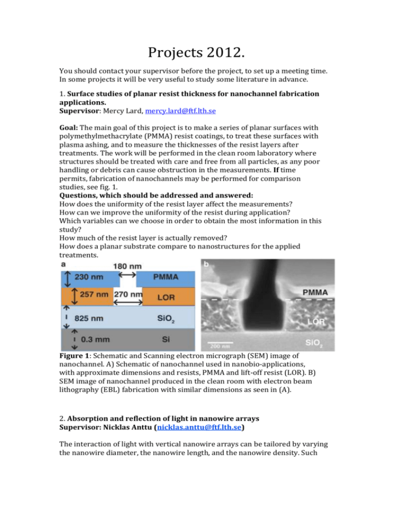
Projects 2012. You should contact your supervisor before the project, to set up a meeting time. In some projects it will be very useful to study some literature in advance. 1. Surface studies of planar resist thickness for nanochannel fabrication applications. Supervisor: Mercy Lard, mercy.lard@ftf.lth.se Goal: The main goal of this project is to make a series of planar surfaces with polymethylmethacrylate (PMMA) resist coatings, to treat these surfaces with plasma ashing, and to measure the thicknesses of the resist layers after treatments. The work will be performed in the clean room laboratory where structures should be treated with care and free from all particles, as any poor handling or debris can cause obstruction in the measurements. If time permits, fabrication of nanochannels may be performed for comparison studies, see fig. 1. Questions, which should be addressed and answered: How does the uniformity of the resist layer affect the measurements? How can we improve the uniformity of the resist during application? Which variables can we choose in order to obtain the most information in this study? How much of the resist layer is actually removed? How does a planar substrate compare to nanostructures for the applied treatments. Figure 1: Schematic and Scanning electron micrograph (SEM) image of nanochannel. A) Schematic of nanochannel used in nanobio-applications, with approximate dimensions and resists, PMMA and lift-off resist (LOR). B) SEM image of nanochannel produced in the clean room with electron beam lithography (EBL) fabrication with similar dimensions as seen in (A). 2. Absorption and reflection of light in nanowire arrays Supervisor: Nicklas Anttu (nicklas.anttu@ftf.lth.se) The interaction of light with vertical nanowire arrays can be tailored by varying the nanowire diameter, the nanowire length, and the nanowire density. Such tunability has great potential to enhance the performance of optoelectronic applications like solar cells, photodetectors and light-emitting diodes. In this project, we measure the reflection of light in absorbing and non-absorbing semiconductor nanowire arrays in order to investigate how the scattering and absorption of light interact to give the optical response of the arrays. If time permits, the optical response will also be modeled with available computer code to enhance the analysis. 3. Electrical conductivity of InP nanowires Supervisor: Gustav Nylund: gustav.nylund@ftf.lth.se We will measure the electrical conductivity of undoped InP nanowires (hopefully with a range of different diameters) and investigate how the conductivity changes with temperature. By using a four-point measurement technique, we can also determine the contact resistance and investigate how/if it changes with temperature and/or diameter. Finally, we will attempt to determine the charge carrier mobility in the nanowires by modulating the conductivity using back-gate voltage sweeps. The first day of this two-day project will be spent in the Lund Nano Lab clean room, processing contacts to individual InP nanowires using electron beam lithography, metal evaporation and lift-off. The second day will be spent doing electrical DC measurements on the fabricated devices using a probe station setup. 4. Calculation of the band-structure of GaAs using k.p-theory Supervisor: Mats-Erik Pistol, mats-erik.pistol@ftf.lth.se In this theory project we will calculate the conduction and valence band structure of GaAs using a quite sophisticated 8-band k.p-model. This is the standard model to calculate bandstructure and is described to some extent in Davies book. We will also include strain in the model to see how the light and heavy hole in the valence band maximum split in energy when we strain the crystal. 5 Growth of GaP Nanowires with AlGaP shell and analyzing by Raman spectroscopy Supervisors: Alexander Berg alexander.berg@ftf.lth.se Mats-Erik Pistol mats-erik.pistol@ftf.lth.se Nanowires are promising for energy efficient devices in the future. In Lund they are mainly grown by MOVPE using gold particles as catalysts. In this project we will grow nanowires in the cleanroom at Lund University (Lund Nano Lab). We will focus on gallium phosphide which might be suitable for optoelectronic devices. After having grown the NWs the gold particles will be etched by wet etching with potassium iodide (KI:H20). Then we can grow a shell containing aluminum gallium phosphide which is quite new and therefore interesting to make research on. The wires will be around 300 nm thick. We will vary the Al/Ga ratio so that the aluminum content does not exceed 30%. As aluminum is very reactive we will grow a very thin GaP shell around it. These wires will be investigated with the scanning electron microscope (SEM). On the second day we will analyze the wires by Raman spectroscopy. 6 Transmission through quantum point contact. Supervisor: Peter Samuelson, samuel@teorfys.lu.se The project concerns a theoretical investigation of electronic transmission through a quantum point contact within the framework of Landauer-Buttiker scattering approach. The quantum point contact in modelled by a saddle point potential [1] for each conduction mode, allowing to analyze the conditions for quantization of conductance [2,3]. [1] M. Buttiker, Phys. Rev. B 41, 7906 (1990). [2] B. J. van Wees et al, Phys. Rev. Lett. 60, 848 (1988). [3] D. A. Wharam et al, J. Phys. C 21, L209 (1988). 7. Investigations of the angular dependence of a nanowire based solar cell. Supervisor: Dan Hessman, dan.hessman@ftf.lth.se In this project we will study a solar cell based on nanowires, which has been fabricated at the department. We will see how the current and voltage from the cell depends on the angle of the incident light. This dependence is a sensitive function of the details of the cell, such as the size and spacing of the nanowires. 8. Electrophoresis of DNA Supervisor: Cassandra Niman, cassandra.niman@ftf.lth.se We will try to cut up DNA with specific and non-specific DNA cutting enzymes and check the products with gel electrophoresis. In this project you will gain experience with handling DNA and also, mixing and running your own gel. We will analyze the results together and talk about other possible applications for this technique. 9 Absorption in quantum wires Supervisor: Arkady Yartsev, arkady.yartsev@chemphys.lu.se Light absorption is one of important characteristics of NW arrays. In general, it is not easy to measure such absorption. Usually, NWs are grown on a nottransparent crystalline substrate, therefore measuring Abs=1-R-T, where R is reflection and T is transmission, is not possible. To resolve a no-transmission problem, we suggest an approach to remove NWs from the substrate by transferring them into a transparent polymer film. Owing to the transferring procedure, NWs do not form large very homogeneous domains in the polymer film. Therefore absorption spectra measured by a conventional absorption spectrometer are disturbed by a relatively strong background signal, which is difficult to evaluate accurately. We suggest using focused probe light beam to accurately measure absorption of relatively small regions of NW-containing polymer films. Such focused probe light method can be utilized by a pair of independently adjustable lenses plugged into a conventional absorption spectrometer. In another approach, you will set an optical fiber-based absorption spectrometer using a fiber-coupled lamp as a wide-band probe light source and a fiber-coupled spectrometer (Ocean Optics) for detection of the transmitted light. You will also consider applicability of the fiber-based set-up for measurements of NWs grown on a substrate in the reflection mode at large incident angles of the probe beam using a bare substrate as a reference sample. Polymer films with embedded InP NWs of various types as well as NWs grown on a substrate are available for measurements. 10. Blinking quantum dots Supervisor: Neimantas Vainorius, neimantasv@gmail.com In this project we will investigate individual quantum dots of InP using photoluminescense. It has been found that these dots blink on a quite long timescale. We will measure a set of these blinking dots and the try to find any statistics of the blinking. We will also see if there are several types of blinkers.
