pip_2354_sm_tableandfigures
advertisement
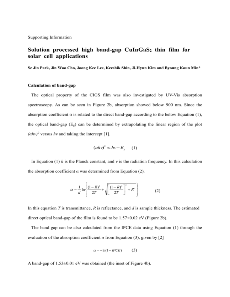
Supporting Information Solution processed high band-gap CuInGaS2 thin film for solar cell applications Se Jin Park, Jin Woo Cho, Joong Kee Lee, Keeshik Shin, Ji-Hyun Kim and Byoung Koun Min* Calculation of band-gap The optical property of the CIGS film was also investigated by UV-Vis absorption spectroscopy. As can be seen in Figure 2b, absorption showed below 900 nm. Since the absorption coefficient α is related to the direct band-gap according to the below Equation (1), the optical band-gap (Eg) can be determined by extrapolating the linear region of the plot (αhv)2 versus hv and taking the intercept [1]. (ahv) 2 hv Eg (1) In Equation (1) h is the Planck constant, and v is the radiation frequency. In this calculation the absorption coefficient α was determined from Equation (2). 2 1 (1 R) 2 (1 R) 2 2 ln R d 2T 2T (2) In this equation T is transmittance, R is reflectance, and d is sample thickness. The estimated direct optical band-gap of the film is found to be 1.57±0.02 eV (Figure 2b). The band-gap can be also calculated from the IPCE data using Equation (1) through the evaluation of the absorption coefficient α from Equation (3), given by [2] ln(1 IPCE ) (3) A band-gap of 1.53±0.01 eV was obtained (the inset of Figure 4b). Figure S1. Thermal gravimetric analysis (TGA) of polyvinyl acetate and CIG paste film Figure S2. Top-view SEM images of Cu, In, and Ga mixed oxide films prepared by the pastes with PVA (a) and ethyl cellulose (b) as a binder material Figure S3. Photoluminescence (PL) spectra of the CIGS film measured at 300 K (excitation source of 355 nm). PL band maximum appears at 810 nm which corresponds to the band-gap of 1.55 eV. Table S1. Electrical properties of the CIGS film Sample Type Carrier concentration (cm-3) CIGS p 9.4×10¹⁶ Mobility (cm2/V·s) Resistivity (Ω·cm) 6.63 10 Figure S4. (a) Top-view SEM image of the CIGS film prepared by the pastes with ethyl cellulose as a binder material and (b) the current density-voltage characteristics of the solar cell device with the CIGS film shown in (a) Reference [1] Woo K, Kim Y, Moon J. A non-toxic, solution-processed, earth abundant absorbing layer for thin-film solar cells. Energy & Environmental Science 2012; 5:5340-5345. [2] Hegedus SS, Shafarman WN. Thin-film solar cells: Device measurements and analysis. Progress in Photovoltaics: Research and Applications 2004; 12(2-3):155-176.
