Report on SEM Secondary electron images and EDX
advertisement
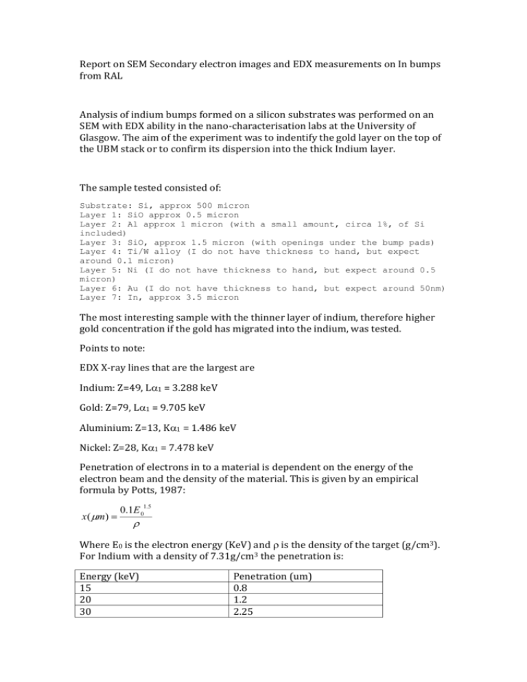
Report on SEM Secondary electron images and EDX measurements on In bumps from RAL Analysis of indium bumps formed on a silicon substrates was performed on an SEM with EDX ability in the nano-characterisation labs at the University of Glasgow. The aim of the experiment was to indentify the gold layer on the top of the UBM stack or to confirm its dispersion into the thick Indium layer. The sample tested consisted of: Substrate: Si, approx 500 micron Layer 1: SiO approx 0.5 micron Layer 2: Al approx 1 micron (with a small amount, circa 1%, of Si included) Layer 3: SiO, approx 1.5 micron (with openings under the bump pads) Layer 4: Ti/W alloy (I do not have thickness to hand, but expect around 0.1 micron) Layer 5: Ni (I do not have thickness to hand, but expect around 0.5 micron) Layer 6: Au (I do not have thickness to hand, but expect around 50nm) Layer 7: In, approx 3.5 micron The most interesting sample with the thinner layer of indium, therefore higher gold concentration if the gold has migrated into the indium, was tested. Points to note: EDX X-ray lines that are the largest are Indium: Z=49, L1 = 3.288 keV Gold: Z=79, L1 = 9.705 keV Aluminium: Z=13, K1 = 1.486 keV Nickel: Z=28, K1 = 7.478 keV Penetration of electrons in to a material is dependent on the energy of the electron beam and the density of the material. This is given by an empirical formula by Potts, 1987: x( m) 0.1E 01.5 Where E0 is the electron energy (KeV) and is the density of the target (g/cm3). For Indium with a density of 7.31g/cm3 the penetration is: Energy (keV) 15 20 30 Penetration (um) 0.8 1.2 2.25 There is also a lateral spread of the electron beam with a similar dependency on the electron beam energy: y( m) 0.077E 01.5 One therefore has to be careful that the electron energy is large enough to allow the L1 of gold to be excited but not too large that the electron beam excites material far from the region of interest. The first measurement was an SEM secondary electron image of the sample, shown in figure 1 and figure 2. These images show that the indium surface is not smooth. There appears to be indium crystals making up the indium bump. Figure 1. SE image of Indium bump on Aluminium pad Figure 2. SE image of Indium bump, Magnification x12 The bump as made was then imaged from above and exposed to an electron beam, with energy between 15 and 30 KeV. The X-ray emission spectrum was taken to understand the elements present. For a beam energy of 15 KeV the elements of oxygen, aluminium and silicon were observed outside of the bump. The bump was sufficiently thick to block the transmission of the 15 KeV electrons from penetrating to the silicon substrate in the area of the bump. The elements of nickel, Indium and gold were observed in the bump region. The results of the elemental maps are shown below. The higher electron beam energy gave a very similar result except that the silicon substrate became visible in the region of the indium bump due to the transmission of the electrons through the indium. Project 1 – Top Illumination EDX on Indium Pad, 15keV electron beam After the top illumination images were made of the bump a Gallium ion beam (FIB) was used to mill away the edge of the bump to allow an image and EDX spectrum to be made of the edge of the bump. A layer of platinum was deposited over the top of the bump to control the edge of the cut section. This is shown in figure 3. Figure 3. Ion beam image of the top of the Indium pad with Platinum strip The area in front of the bump was removed, shown in figure 4. The sample was rotate by 52o and imaged with the SEM as a secondary electron image. A series of images were made a different magnification (figures 5 to 8 for magnifications from 10x to 50x). The images shows the 0.5 um thick SiO2 layer with the 1 um thick Aluminium layer on top of this. There is a 1.5 um thick SiO2 layer which defines the area of the Indium bump. On top of the Aluminium layer is a 400 nm thick metal layer. This includes, in contact with the aluminium layer, an approximately 100nm thick Ti/W alloy layer. The Ti/W layer can be seen in the images as a bright line. The majority of this 400nm thick layer is nickel. On the top of the nickel layer was deposited 50nm of Gold. Gold gives an anomalously high secondary electron emission yield and one would therefore expect to see a bight line on the top of the nickel layer (especially in figure 8). This is not visible and as a result one might conclude that the gold is no longer present in a welldefined layer. The SEM images show the shape of the Indium layer. This is clearly not flat. It has a raised edge with a significant dip in the middle. Small crystal type structures and what appear to be voids in the Indium bulk are visible. It should be noted that there is a layer of platinum on the top of the Indium bump at the edge which appears as metal with full fill factor. Figure 4. Ion beam image of top of bump with half the bump milled away Figure 5. SEM image of side view (52deg) of Indium bump, Mag 10x Figure 6. SEM image of side view (52deg) of Indium bump, Mag 15x Figure 7. SEM image of side view (52deg) of Indium bump, Mag 20x Figure 8. SEM image of side view (52deg) of Indium bump, Mag 50x EDX spectra were made of the bump with side illumination, with the angle of incidence at 52 degrees. The electron beam energy was 15keV to reduce penetration into the material and scatter sideways. Three EDX spectra were obtained at three points using the point measure function. These were in the Indium layer (spectrum 1, figures 9 and 10), in the Indium layer near the bottom of the indium layer (spectrum 2, figures 11 and 12) and in the Nickel UBM layer near the bottom of this layer (spectrum 3, figure 13). Spectrum 3 (illumination at the bottom of the UBM stack) showed a significant percentage of Si, O and Al as the electron beam penetrated the nickel layer and entered the underlying materials, some Nickel was identified. No gold was identified as expected for these layers. Spectrum 2 showed a stronger nickel content at 35% by weight. Indium made up 25% by weight and the remainder was attributed to Boron, which might be present in silicon or a miss identification of a low atomic number material. The spectrum 3, which was obtained from a point in the indium but further from the nickel layer, has a higher percentage of indium as expected, (50%). Nickel contributed the third highest percentage by weight (16%). Platinum contributed to the EDX spectra (18% by weight) due to lateral scatter into the platinum top layer. Gold was identified in the spectra by telling the software to expect gold and to fit to this. Without user intervention the software did not identify gold automatically. Visual inspection of the spectra did not show any obvious peaks at the energy of gold and this assignment of gold may be in error. Gold was found at the 3% level by weight. The expected thickness of the gold layer is 50nm and the Indium layer is measured to be about 2um. This would imply a concentration of gold at 3.9% in the indium by weight if all the gold dissolved into the indium. Given that Indium made up 50% of the sample from the spectra then gold should make up 2% of the sample from the spectra, by weight. Therefore a number of 3% obtained is consistent with that expected and supports the hypothesis that the gold has migrated into the indium. Figure 9. Position EDX spectra 1 was obtained Figure 10. EDX Spectra from spectrum point 1 above Spectrum 1 processing : Peaks possibly omitted : 15.580, 16.451, 17.000 keV Processing option : All elements analyzed (Normalised) Number of iterations = 3 Standard : O SiO2 1-Jun-1999 12:00 AM Si SiO2 1-Jun-1999 12:00 AM Ni Ni 1-Jun-1999 12:00 AM Ga GaP 1-Jun-1999 12:00 AM In InAs 1-Jun-1999 12:00 AM Pt Pt 1-Jun-1999 12:00 AM Au Au 1-Jun-1999 12:00 AM Element Weight% Atomic% OK 1.92 10.03 Si K 4.87 14.51 Ni K 15.93 22.71 Ga L 6.09 7.31 In L 49.77 36.27 Pt M 18.28 7.84 Au M 3.13 1.33 Totals 100.00 Figure 11. Position EDX spectra 2 was obtained Figure 12. EDX Spectra from spectrum point 2 above Spectrum 2 processing : No peaks omitted Processing option : All elements analyzed (Normalised) Number of iterations = 4 Standard : B B 20-Jul-1999 12:00 AM O SiO2 1-Jun-1999 12:00 AM Al Al2O3 1-Jun-1999 12:00 AM Si SiO2 1-Jun-1999 12:00 AM Ni Ni 1-Jun-1999 12:00 AM Ga GaP 1-Jun-1999 12:00 AM Zr Zr 1-Jun-1999 12:00 AM In InAs 1-Jun-1999 12:00 AM Au Au 1-Jun-1999 12:00 AM Element Weight% Atomic% BK 26.66 65.80 OK 1.44 2.41 Al K 4.52 4.47 Si K 4.99 4.75 Ni K 34.77 15.81 Ga L 2.21 0.85 Zr L 0.78 0.23 In L 24.34 5.66 Au M 0.28 0.04 Totals 100.00 Figure 13. EDX Spectra from spectrum point 3 taken inside the Indium layer and away from the UBM. Spectrum 3 processing : No peaks omitted Processing option : All elements analyzed (Normalised) Number of iterations = 3 Standard : O SiO2 1-Jun-1999 12:00 AM Al Al2O3 1-Jun-1999 12:00 AM Si SiO2 1-Jun-1999 12:00 AM Mn Mn 1-Jun-1999 12:00 AM Ni Ga Ni 1-Jun-1999 12:00 AM GaP 1-Jun-1999 12:00 AM Se Se 1-Jun-1999 12:00 AM In InAs 1-Jun-1999 12:00 AM Element Weight% Atomic% OK 10.69 18.28 Al K 47.89 48.56 Si K 28.63 27.89 Mn K 0.02 0.01 Ni K 7.17 3.34 Ga L 2.52 0.99 Se L 1.89 0.65 In L 1.18 0.28 Totals 100.00 An EDX spectra was obtained for an area that included the Indium bump, the UBM layers and the Aluminum. The indium bump is in the lower half of the scanned area and the UBM at the top of the scanned area. Again the sample was illuminated at 52degrees. The results are shown below. The elements of Oxygen, Silicon, Nickel, Indium, Platinum and Gold were identified. There is some localization of the different materials within the area scanned. The Oxygen and silicon are present throughout the scanned area, which maybe due to the penetration of the beam into the sample and the excitation of the substrate under the indium, given that the illumination was not normal to the surface. Indium is only visible in the lower half of the scanned area as would be expected. Nickel is visible in the lower half but extends higher up into the scanned area than the Indium. Again this is as expected. Platinum is visible due to the platinum bar at the top of the indium due to scatter. Finally gold was detected in the sample. The gold was detected only in the lower half of the scanned area; this is consistent with the gold being distributed in the indium material. Project 1. EDX spectrum over a limited area of Indium and UBM In summary the SEM secondary emission electron images and the EDX images taken of the cross-section of the Indium bump on a UBM layer indicated the absences of a 50nm gold layer between the indium and the Nickel of the UBM. It is probable that the gold has become re-distributed inside the indium. Gold has been detected, all be it with some effort and perhaps at the lower detection limit of the apparatus, inside the indium bump using the EDX technique.
