Metamaterial Absorber/Emitter Based on Nanowire Cavities for
advertisement
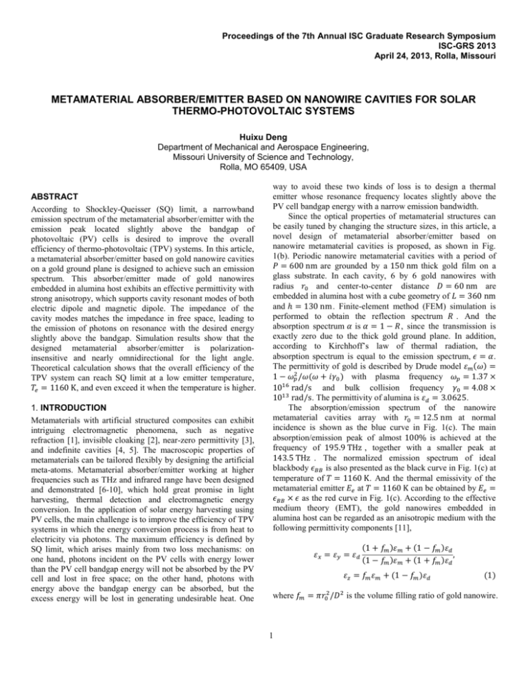
Proceedings of the 7th Annual ISC Graduate Research Symposium ISC-GRS 2013 April 24, 2013, Rolla, Missouri METAMATERIAL ABSORBER/EMITTER BASED ON NANOWIRE CAVITIES FOR SOLAR THERMO-PHOTOVOLTAIC SYSTEMS Huixu Deng Department of Mechanical and Aerospace Engineering, Missouri University of Science and Technology, Rolla, MO 65409, USA ABSTRACT According to Shockley-Queisser (SQ) limit, a narrowband emission spectrum of the metamaterial absorber/emitter with the emission peak located slightly above the bandgap of photovoltaic (PV) cells is desired to improve the overall efficiency of thermo-photovoltaic (TPV) systems. In this article, a metamaterial absorber/emitter based on gold nanowire cavities on a gold ground plane is designed to achieve such an emission spectrum. This absorber/emitter made of gold nanowires embedded in alumina host exhibits an effective permittivity with strong anisotropy, which supports cavity resonant modes of both electric dipole and magnetic dipole. The impedance of the cavity modes matches the impedance in free space, leading to the emission of photons on resonance with the desired energy slightly above the bandgap. Simulation results show that the designed metamaterial absorber/emitter is polarizationinsensitive and nearly omnidirectional for the light angle. Theoretical calculation shows that the overall efficiency of the TPV system can reach SQ limit at a low emitter temperature, 𝑇𝑒 = 1160 K, and even exceed it when the temperature is higher. 1. INTRODUCTION Metamaterials with artificial structured composites can exhibit intriguing electromagnetic phenomena, such as negative refraction [1], invisible cloaking [2], near-zero permittivity [3], and indefinite cavities [4, 5]. The macroscopic properties of metamaterials can be tailored flexibly by designing the artificial meta-atoms. Metamaterial absorber/emitter working at higher frequencies such as THz and infrared range have been designed and demonstrated [6-10], which hold great promise in light harvesting, thermal detection and electromagnetic energy conversion. In the application of solar energy harvesting using PV cells, the main challenge is to improve the efficiency of TPV systems in which the energy conversion process is from heat to electricity via photons. The maximum efficiency is defined by SQ limit, which arises mainly from two loss mechanisms: on one hand, photons incident on the PV cells with energy lower than the PV cell bandgap energy will not be absorbed by the PV cell and lost in free space; on the other hand, photons with energy above the bandgap energy can be absorbed, but the excess energy will be lost in generating undesirable heat. One way to avoid these two kinds of loss is to design a thermal emitter whose resonance frequency locates slightly above the PV cell bandgap energy with a narrow emission bandwidth. Since the optical properties of metamaterial structures can be easily tuned by changing the structure sizes, in this article, a novel design of metamaterial absorber/emitter based on nanowire metamaterial cavities is proposed, as shown in Fig. 1(b). Periodic nanowire metamaterial cavities with a period of 𝑃 = 600 nm are grounded by a 150 nm thick gold film on a glass substrate. In each cavity, 6 by 6 gold nanowires with radius 𝑟0 and center-to-center distance 𝐷 = 60 nm are embedded in alumina host with a cube geometry of 𝐿 = 360 nm and ℎ = 130 nm. Finite-element method (FEM) simulation is performed to obtain the reflection spectrum 𝑅 . And the absorption spectrum 𝛼 is 𝛼 = 1 − 𝑅, since the transmission is exactly zero due to the thick gold ground plane. In addition, according to Kirchhoff’s law of thermal radiation, the absorption spectrum is equal to the emission spectrum, 𝜖 = 𝛼. The permittivity of gold is described by Drude model 𝜀𝑚 (𝜔) = 1 − 𝜔𝑝2 /𝜔(𝜔 + 𝑖𝛾0 ) with plasma frequency 𝜔𝑝 = 1.37 × 10¹⁶ rad/s and bulk collision frequency 𝛾0 = 4.08 × 10¹³ rad/s. The permittivity of alumina is 𝜀𝑑 = 3.0625. The absorption/emission spectrum of the nanowire metamaterial cavities array with 𝑟0 = 12.5 nm at normal incidence is shown as the blue curve in Fig. 1(c). The main absorption/emission peak of almost 100% is achieved at the frequency of 195.9 THz , together with a smaller peak at 143.5 THz . The normalized emission spectrum of ideal blackbody 𝜖𝐵𝐵 is also presented as the black curve in Fig. 1(c) at temperature of 𝑇 = 1160 K. And the thermal emissivity of the metamaterial emitter 𝐸𝑒 at 𝑇 = 1160 K can be obtained by 𝐸𝑒 = 𝜖𝐵𝐵 × 𝜖 as the red curve in Fig. 1(c). According to the effective medium theory (EMT), the gold nanowires embedded in alumina host can be regarded as an anisotropic medium with the following permittivity components [11], 𝜀𝑥 = 𝜀𝑦 = 𝜀𝑑 (1 + 𝑓𝑚 )𝜀𝑚 + (1 − 𝑓𝑚 )𝜀𝑑 , (1 − 𝑓𝑚 )𝜀𝑚 + (1 + 𝑓𝑚 )𝜀𝑑 𝜀𝑧 = 𝑓𝑚 𝜀𝑚 + (1 − 𝑓𝑚 )𝜀𝑑 (1) where 𝑓𝑚 = 𝜋𝑟02 /𝐷2 is the volume filling ratio of gold nanowire. 1 Figure 1. Schematic of the TPV system and the emission spectra of the metamaterial emitter. (a) is the TPV system model mainly including three components: the heat source to provide thermal energy, metamaterial absorber/emitter to emit photons at the specific frequency and the PV cell to collect photons and generate electricity. (b) is the structure of the metamaterial absorber/emitter made of gold nanowires embedded in alumina host. (c) is the emission spectra in which the black curve is the normalized emissivity of ideal blackbody 𝜖𝐵𝐵 at 𝑇 = 1160 K, the blue curve is the emissivity of the metamaterial absorber/emitter 𝜖 which is equal to its absorptivity according to Kirchhoff’s law, 𝜖 = 𝛼, and the red curve is the thermal emission spectrum of the emitter, 𝐸𝑒 = 𝜖𝐵𝐵 × 𝜖 at 𝑇 = 1160 K. The PV cell can absorb photons with energy higher than the bandgap 𝐸𝑔 represented by the yellow area. 2. ANALYSIS OF THE ABSORBER/EMITTER The magnetic field profiles 𝐻𝑦 in the x-z plane of the cavity resonant modes are shown in Fig. 2(c,d), where the 𝑚 = 1 mode with one magnetic field peak along the x direction is located at the main absorption/emission peak; while the 𝑚 = 3 mode corresponds to the weak absorption/emission resonance . In the x-y plane as shown in Fig. 2(a,b), the magnetic field profiles are homogeneous along the y direction for both modes. The 𝑚 = 2 mode is absent at the normal incidence due to the structural mirror symmetry (with respect to y-z plane) of the metamaterial cavities. The mechanism of high emission for the 𝑚 = 1 mode can be understood as the cavity mode supports the electric dipole resonance and the magnetic dipole resonance simultaneously. As shown in Fig. 2(e), the divergence and convergence of electric field at the top left and top right corners of the metamaterial cavity imply the accumulation of polarized positive charges and negative charges (with ∇ ∙ 𝐸⃗ = 𝜌/𝜀0 , where 𝜌 is the polarized charge density), which serves as a strong electric dipole. Fig. 2(f) shows the distribution of displacement current 𝐷 , with 𝜕𝐷/𝜕𝑡 = −𝑖𝜔𝐷 = −𝑖𝜔𝜀𝐸 . Strong displacement current is found inside the grounded gold film due to the large negative permittivity of metal. Anti-parallel displacement currents are formed between the nanowire cavity and the gold ground plane, resulting in a strong magnetic dipole resonance, which is also shown in Fig. 2(f). The presence of both electric resonance and magnetic resonance can result in matched impedance to the free space, i.e., high absorption/emission of photons on resonance. The current absorber/emitter works in a narrow bandwidth due to the resonance nature of light absorption/emission. To ensure the emission resonant frequency is slightly above the bandgap energy for different PV cells, the geometries of the absorber/emitter structures can be tuned accordingly. Since the impedance matching condition is critical for obtaining high absorption/emission, it is expected that 𝑓𝑚 will largely affect the performance of the metamaterial Figure 2. (a) and (b) are the magnetic field profiles of the m = 1 and m = 3 resonant modes in the x-y plane, respectively; while (c) and (d) are in the x-z plane. (e) is the intensity and direction of the electric field and (d) is the displacement current for 𝑚 = 1 mode at 𝑦 = 0. absorber/emitter. Fig. 3(a,b) shows the dependence of absorption/emission spectra on 𝑓𝑚 at incident angle 𝜃 = 0° with different collision frequencies of gold 𝛾, where the variation of filling ratio is derived by tuning the radius of the gold nanowires from 𝑟0 = 10 nm to 𝑟0 = 20 nm. Considering that the collision 2 frequency 𝛾 increases a lot due to the inevitable surface roughness of the fabricated sample, numerical simulations with 𝛾 = 𝛾0 and 𝛾 = 3𝛾0 are shown in Fig. 3(a) and Fig. 3(b), respectively. For 𝛾 = 𝛾0 , the main absorption/emission peak is obtained around 𝑓𝑚 = 0.14 . For 𝛾 = 3𝛾0 , the highest absorption/emission occurs at a larger filling ratio around 𝑓𝑚 = 0.25. The absorption/emission spectra of 𝛾 = 3𝛾0 show much broader bandwidth compared to those of 𝛾 = 𝛾0 . By comparing the absorption/emission spectra of the two collision frequencies, it is also found that the resonance for the 𝑚 = 3 mode becomes much weaker at 𝛾 = 3𝛾0 since high order resonance is very sensitive to the material loss. Besides, there is an additional resonance peak between the 𝑚 = 1 and the 𝑚 = 3 modes at large filling ratios (𝑓𝑚 > 0.22) when 𝛾 = 𝛾0 . This is a high order mode oscillating along the y direction. 𝜃 increases, while the peak remains the same. The absorption/emission of TM polarized light, on the other hand, decreases in a slower way than that of TE polarized light, while the peak slightly shifts with the growth of incident angle. Nevertheless, the absorption/emission remains strong for incident angle up to 80° for both polarizations. An additional peak is noted for incident angle larger than 40° in Fig. 3(d) and 3(f), which is the 𝑚 = 2 mode excited by the oblique incident light. 3. EFFICIENCY OF THE TPV SYSTEM To evaluate the performance of the metamaterial emitter made of nanowire cavities for TPV systems, the overall system efficiency is theoretically calculated. In general, the maximum efficiency of TPVs is limited by the Carnot efficiency (all heat energy is converted to electrical energy without loss) which can be given by 𝜂𝑐𝑎𝑟 = 1 − 𝑇𝑐 /𝑇𝑒 . When the temperature of the PV cell collector is 300 K and the temperature of the emitter is maintained at 1000 K , a maximum efficiency of 0.7 can be obtained. However, for TPV systems, efficiencies are limited by other factors in the energy conversion process from heat to electricity via photons. Following the analysis by Shockley and Queisser, the overall energy conversion efficiency for TPVs is limited by [12] 𝜂 = 𝑈(𝑇, 𝐸𝑔 ) × 𝜈(𝑇, 𝐸𝑔 ) × 𝑚(𝑉𝑜𝑝 ) Figure 3. (a) and (b) are the dependence of absorption spectra on metal filling ratio at normal incidence with different collision frequencies of gold, 𝛾 = 𝛾0 and 𝛾 = 3𝛾0 , respectively. (c-f) are the dependence of light absorption on the incident angle 𝜃 for different polarizations and collision frequencies with 𝑓𝑚 = 0.14 in (c, d) and 𝑓𝑚 = 0.25 in (e, f). Since the metamaterial cavities array possesses 4-fold rotation symmetry in the x-y plane, it is polarizationindependent at normal incidence. For oblique incidence, however, the absorption/emission performance will depends on the polarization. The absorption/emission spectra for both polarizations (transverse electric (TE) polarization and transverse magnetic (TM) polarization) at two different collision frequencies are shown in Fig. 3(c-f). The absorption/emission of TE polarized light will decrease gradually as the incident angle (2) where 𝑈 is the so-called ‘ultimate efficiency’ which is proportional to the energy contained in photon-excited electronhole pairs divided by the incident radiation energy, 𝜈 is an efficiency due to recombination process which means charge carries may be removed from the PV cell in additional ways, and finally 𝑚 is called ‘impedance mismatch’ efficiency caused by the difference between the open circuit voltage 𝑉𝑜𝑝 and the optimal operating voltage. According to the assumption that one photon with energy larger than the PV cell energy gap 𝐸𝑔 will excite one electronhole pair resulting in a contribution of 𝐸𝑔 electricity energy to the TPV system, the ultimate efficiency can be achieved by calculating the energy carried by excited electron-hole pairs with respect to the incident radiation energy [12, 13]: 𝜋/2 𝑈= ∫0 ∞ 𝑑𝜃 sin(2𝜃) ∫𝐸 𝑑𝐸𝜖(𝐸, 𝜃)𝐼𝐵𝐵 (𝐸, 𝑇𝑒 ) 𝑔 𝜋/2 ∫0 ∞ 𝐸𝑔 𝐸 𝑑𝜃 sin(2𝜃) ∫0 𝑑𝐸𝜖(𝐸, 𝜃)𝐼𝐵𝐵 (𝐸, 𝑇𝑒 ) (3) In this equation, the denominator is the incident radiation energy onto the PV cell, which is equal to the thermal emission energy from the metamaterial emitter calculated by the integral of blackbody radiation 𝐼𝐵𝐵 (when the emitter temperature is 𝑇𝑒 ) multiplying the emission of the emitter at all angles 𝜃 (assuming the emitter to be planar with no azimuthal angular dependence). The numerator is the energy contained in excited electron-hole pairs by cutting off the photon energy below 𝐸𝑔 and reducing the higher photon energy into 𝐸𝑔 . In order to average the 3 Figure 4. Theoretical calculation of the TPV system efficiency as a function of the PV cell bandgap energy 𝐸𝑔 and the emitter temperature 𝑇𝑒 . (a) is the ultimate efficiency 𝑈, which is optimized when either of the two resonance peaks (195.9 THz → 0.8 eV and 143.5 THz → 0.59 eV) of the emission spectrum is slightly above the bandgap 𝐸𝑔 . The dashed line represents the bandgap energy of GaSb, 𝐸𝑔 = 0.71 eV. (b) and (c) are the recombination efficiency 𝜈 and the impedance mismatch efficiency 𝑚 , respectively, which will decrease when the emitter temperature is decreased. (d) is the overall conversion efficiency, 𝜂 = 𝑈 × 𝜈 × 𝑚, which can reach the SQ limit of 0.31 when the PV cell is GaSb (represented by the horizontal dashed line, 𝐸𝑔 = 0.71 eV) and the temperature is relatively low (represented by the vertical dashed line, 𝑇𝑒 = 1160 K). emission in both TE and TM polarizations, we take 𝜖(𝐸, 𝜃) = 𝜖 𝑇𝐸 (𝐸, 𝜃)/2 + 𝜖 𝑇𝑀 (𝐸, 𝜃)/2. Besides the efficiency of creating excited electron-hole pairs, the recombination efficiency 𝜈 is utilized to measure the percent of charge carriers becoming the desired external current. And it can be expressed as the ratio between the open circuit voltage 𝑉𝑜𝑝 and the initial material bandgap voltage 𝑉𝑔 = 𝐸𝑔 /𝑞, in which 𝑞 is the charge of one electron [13, 14]: 𝑉𝑜𝑝 𝑉𝑐 𝑄𝑒 (𝑇, 𝐸𝑔 ) 𝜈= = ln (𝑓 ) 𝑉𝑔 𝑉𝑔 𝑄𝑐 (𝑇𝑐 , 𝐸𝑔 ) (4) where 𝑉𝑐 = 𝑘𝐵 𝑇𝑐 /𝑞 is the voltage of the PV cell related to the cell temperature 𝑇𝑐 . 𝑄𝑒 and 𝑄𝑐 are photon number flux incident on the PV cell from the emitter, and from an ideal blackbody surrounding the cell at the same temperature of the PV cell 𝑇𝑐 , respectively, as shown in Eq. (5) [13]. Here, 𝑓 is chosen as 0.5 for an ideal case when both the emitter and the cell have planar geometries. 𝜋 ∞ 2𝜋 2 𝐸 2 𝑑𝐸 𝑄𝑒 (𝑇, 𝐸𝑔 ) = 3 2 ∫ sin(2𝜃) 𝑑𝜃 ∫ 𝜖𝑒 (𝐸, 𝜃) , 𝐸 ℎ 𝑐 0 𝐸𝑔 exp ( )−1 𝑘𝐵 𝑇 2𝜋 ∞ 𝐸 2 𝑑𝐸 𝑄𝑐 (𝑇𝑐 , 𝐸𝑔 ) = 3 2 ∫ (5) ℎ 𝑐 𝐸𝑔 exp ( 𝐸 ) − 1 𝑘𝐵 𝑇𝑐 The third factor in Eq. (2), 𝑚(𝑉𝑜𝑝 ), is evaluated when the operating voltage 𝑉𝑚𝑎𝑥 is chosen to maximize the electrical power for the PV cell and given by Ref. [13]: 𝑚(𝑉𝑜𝑝 ) = 2 𝑧𝑚 (1 + 𝑧𝑚 − 𝑒 −𝑧𝑚 )(𝑧𝑚 + ln(1 + 𝑧𝑚 )) (6) with 𝑧𝑚 determined by the ratio between 𝑉𝑚𝑎𝑥 and 𝑉𝐶 , and related to 𝑧𝑜𝑝 = 4 𝑉𝑜𝑝 = 𝑧𝑚 + ln(1 + 𝑧𝑚 ) 𝑉𝑐 (7) When the filling ratio of nanowire in the emitter is 𝑓𝑚 = 0.14 and the collision frequency of gold is 𝛾 = 𝛾0 as shown in Fig. 3(c,d), each efficiency factor in Eq. (2), 𝑈, 𝜈 and 𝑚, is calculated and plotted in Fig. 4, as functions of the PV cell bandgap energy 𝐸𝑔 and the temperature of the emitter 𝑇𝑒 . While 𝜈 and 𝑚 are both determined by the PV cell properties, 𝑈 is enhanced by the designed metamaterial emitter so that the overall efficiency of the TPV system is improved. From Fig. 4(d), the maximum efficiency locates at 𝐸𝑔 = 0.7~0.8 eV , where the resonance of the emitter (195.9 THz corresponding to 0.8 eV) is slightly above the bandgap energy 𝐸𝑔 . As mentioned above, the explanation is that photons with energy below 𝐸𝑔 cannot be absorbed by the PV cell, however, for the photons with energy above 𝐸𝑔 , the additional energy ∆𝐸 = 𝐸 − 𝐸𝑔 is lost to thermalization within the PV cell. Here, the resonance of the emitter is tuned at 195.9 THz by changing the filling ratio to well match the gallium antimonide (GaSb) PV cell with a bandgap energy of 0.71 eV . In this case, the needed emitter temperature is about 𝑇𝑒 ≈ 1160 K to reach the SQ limit, 𝜂𝑆𝑄 = 0.31. This temperature is much lower than that in practical solar TPV systems which is less than 2500 K. If the temperature is too low, the efficiency will decrease due to the decrease of 𝜈 and 𝑚. When the temperature increases, the efficiency can even get higher and exceed the SQ limit, but it is limited by the melting point of the emitter materials [15]. The melting temperature of gold is around 1337 K, which is much lower than the current operation temperature of 1160 K. Therefore, new designs of the emitter with high melting point materials may be possible to improve the overall efficiency furthermore at high temperature. 4. CONCLUSIONS In conclusion, in order to improve the overall efficiency of TPV system, a metamaterial absorber/emitter based on nanowire cavities is proposed and demonstrated. The cavity resonant mode with mode order 𝑚 = 1 is utilized to excite both the electric dipole and the magnetic dipole simultaneously. At a specific frequency, the impedance of the metamaterial absorber/emitter can match to the free space, and the strong optical loss in nanowire structures results in high emissivity with narrow emission bandwidth. The resonant frequency can be tuned to match the bandgap energy of different PV cells by changing the filling ratio of gold nanwires. The absorption/emission depending on different incident angles for both the TE and TM polarizations is also investigated and utilized in calculating the efficiency of TPV systems. The overall conversion efficiency consists of three parts: the ultimate efficiency 𝑈, the recombination efficiency 𝜈 and the impedance mismatch efficiency 𝑚 . By tuning the emission resonant frequency slightly above the PV cell bandgap energy, the overall efficiency can reach SQ limit 𝜂𝑆𝑄 = 0.31 at a low temperature of 1160 K. When the temperature of the emitter is increased, the efficiency can exceed the SQ limit, but it is still limited by the melting point of the emitter materials. 5. ACKNOWLEDGEMENTS This work was partially supported by the Department of Mechanical and Aerospace Engineering, and the Intelligent Systems Center at Missouri S&T. The authors thank Y. He and J. Gao for helpful discussions. 6. REFERENCES [1] Shelby, R.A., D.R. Smith, and S. Schultz, 2001, "Experimental Verification of a Negative Index of Refraction," Science, 292(5514): pp. 77-79. [2] Pendry, J.B., D. Schurig, and D.R. Smith, 2006, "Controlling Electromagnetic Fields," Science, 312(5781): pp. 1780-1782. [3] Alù, A., et al., 2007, "Epsilon-near-zero metamaterials and electromagnetic sources: Tailoring the radiation phase patter," Physical Review B, 75(15): pp. 155410. [4] Yao, J., et al., 2011, "Three-dimensional nanometer-scale optical cavities of indefinite medium," Proceedings of the National Academy of Sciences, 108(28): pp. 11327-11331. [5] Yang, X., et al., 2012, "Experimental realization of threedimensional indefinite cavities at the nanoscale with anomalous scaling laws," Nat Photon, 6(7): pp. 450-454. [6] Tao, H., et al., 2008, "A metamaterial absorber for the terahertz regime: design, fabrication and characterization," Opt. Express, 16(10): pp. 7181-7188. [7] Liu, N., et al., 2010, "Infrared Perfect Absorber and Its Application As Plasmonic Sensor," Nano Letters, 10(7): pp. 2342-2348. [8] Avitzour, Y., Y.A. Urzhumov, and G. Shvets, 2009, "Wide-angle infrared absorber based on a negative-index plasmonic metamaterial," Physical Review B, 79(4): pp. 045131. [9] Liu, X., et al., 2011, "Taming the Blackbody with Infrared Metamaterials as Selective Thermal Emitters," Physical Review Letters, 107(4): pp. 045901. [10] Cui, Y., et al., 2012, "Ultrabroadband Light Absorption by a Sawtooth Anisotropic Metamaterial Slab," Nano Letters, 12(3): pp. 1443-1447. [11] Sihvola, A., 1999, "Electromagnetic Mixing Formulae and Applications," Institution of Electrical Engineers. [12] Shockley, W. and H.J. Queisser, 1961, "Detailed Balance Limit of Efficiency of p-n Junction Solar Cells," Journal of Applied Physics, 32(3): pp. 510-519. [13] Rephaeli, E. and S. Fan, 2009, "Absorber and emitter for solar thermo-photovoltaic systems to achieve efficiency exceeding the Shockley-Queisser limit," Opt. Express, 17(17): pp. 15145-15159. [14] Chihhui, W., et al., 2012, "Metamaterial-based integrated plasmonic absorber/emitter for solar thermo-photovoltaic systems," Journal of Optics, 14(2): pp. 024005. [15] Molesky, S., Dewalt, C. J., and Jacob, Z., 2013, "High temperature epsilon-near-zero and epsilon-near-pole metamaterial emitters for thermophotovoltaics," Opt. Express 21, A96-A110. 5

