Photolithography and Etching in Nanometer
advertisement
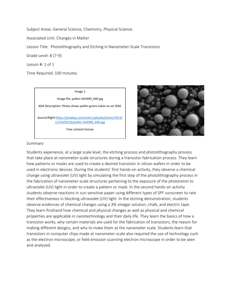
Subject Areas: General Science, Chemistry, Physical Science. Associated Unit: Changes in Matter Lesson Title: Photolithography and Etching in Nanometer-Scale Transistors Grade Level: 8 (7-9) Lesson #: 1 of 1 Time Required: 100 minutes. Image 1 Image file: pollen-543490_640.jpg ADA Description: Photo shows pollen grains taken on an SEM. Source/Right:https://pixabay.com/static/uploads/photo/2014/ 11/24/03/16/pollen-543490_640.jpg Free content license Summary Students experience, at a large scale level, the etching process and photolithography process that take place at nanometer-scale structures during a transistor fabrication process. They learn how patterns or masks are used to create a desired transistor in silicon wafers in order to be used in electronic devices. During the students’ first hands-on activity, they observe a chemical change using ultraviolet (UV) light by simulating the first step of the photolithography process in the fabrication of nanometer-scale structures pertaining to the exposure of the photoresist to ultraviolet (UV) light in order to create a pattern or mask. In the second hands-on activity students observe reactions in sun-sensitive paper using different types of SPF sunscreen to rate their effectiveness in blocking ultraviolet (UV) light. In the etching demonstration, students observe evidences of chemical changes using a 3% vinegar solution, chalk, and electric tape. They learn firsthand how chemical and physical changes as well as physical and chemical properties are applicable in nanotechnology and their daily life. They learn the basics of how a transistor works, why certain materials are used for the fabrication of transistors, the reason for making different designs, and why to make them at the nanometer scale. Students learn that transistors in computer chips made at nanometer-scale also required the use of technology such as the electron microscope, or field emission scanning electron microscope in order to be seen and analyzed. Engineering Connection: Engineers working with nanoparticles must fully understand chemical and physical changes of matter in order to apply these concepts in the design, fabrication, and transportation of nanometer-scale structures. A chemical change implies a chemical reaction, and engineers need to understand the properties of elements and compounds in order to be able to create desired transistors or custom products containing nanometer-scale substances by prompting or inhibiting chemical changes in matter. In the case of nanometer-scale transistors, engineering and researchers look for ways of creating, blocking or narrowing routes for electrons to flow using chemical and physical means. Engineers apply concepts of chemical reactions as well as biological reactions that take place with atoms, molecules, fluids and organs in our bodies, in order to imitate the concepts and behaviors to improve our quality of life and advancements in technology. Engineers rely on technology to develop new and enhanced computer chips at the nanometer scale, a human eye is not able to see features outside of the visible light wavelength; they need to use special devices such as the electron microscope, or the field emission scanning electron microscope which allow them to see features at this level. Training is required in order to use these devices. Engineering Category 1. Relating science concepts to engineering. Keywords Chemical change, etching, mask, nanometer, nanotechnology, mask, photolithography, photoresist, physical change, transistor, UV light, wafer. Educational Standards State STEM Standard: https://www.teachengineering.org/search_standards.php?select_state=Florida&catsat=true&id= S1130818 (source) Big Idea 9: Changes in Matter (K-8) Current Standard • Differentiate between physical changes and chemical changes. (8-8) (no curriculum aligned) Big Idea 1: The Practice of Science (K-8) Current Standard: • Understand that scientific investigations involve the collection of relevant empirical evidence, the use of logical reasoning, and the application of imagination in devising hypotheses, predictions, explanations, and models to make sense of the collected evidence. (8-8) ITEEA Standard Standard 1: Students will develop an understanding of the characteristics and scope of technology. F. New products and systems can be developed to solve problems or to help do things that could not be done without the help of technology. Standard 2. Students will develop an understanding of the core concepts of technology. T. Different technologies involve different sets of processes. Standard 3. Students will develop an understanding of the relationships among technologies and the connections between technology and other fields of study. F. Knowledge gained from other fields of study has a direct effect on the development of technological products and systems. NGSS Standard LAFS.68.RST.3.9: Compare and contrast the information gained from experiments, simulations, videos, or other multimedia sources, with the information gained from reading a text on the same topic. LAFS.68.WHST.2.4: Produce clear and coherent writings in which the development, organization, and style are appropriate to the task, purpose, and audience. LAFS.68.WHST.3.7: Conduct short research projects to answer a question (including a selfgenerated question), drawing from several sources and generating additional related, focused questions that allow for multiple avenues of exploration. SC.8.P.8.4: Classify and compare substances on the basis of characteristic physical properties that can be demonstrated or measured, for example: density, thermal or electrical conductivity, solubility, magnetic properties, or melting and boiling points, and know that these properties are independent of the amount of the sample. SC.8.P.9.2: Differentiate between physical changes and chemical changes. SC.8.N.1.1: Define a problem from the eighth grade curriculum using appropriate reference materials to support scientific understanding, plan and carry out scientific investigations of various types such as systematic observations or of experiments, identify variables, collect and organize data, interpret data in charts, tables, and graphics, analyze information, make predictions, and defend conclusions. SC.8.N.1.3: Use phrases such as "results support" or "fail to support" in science, understanding that science does not offer conclusive 'proof' of a knowledge claim. MAFS.8.EE.2.5 Graph proportional relationships, interpreting the unit rate as the slope of the graph. Compare two different proportional relationships represented in different ways. For example: compare a distance-time graph to a distance-time equation to determine which of two moving objects has greater speed. MAFS.8.F.2.5 Describe qualitatively the functional relationship between two quantities by analyzing a graph (e.g., where the function is increasing or decreasing, linear or nonlinear). Sketch a graph that exhibits the qualitative features of a function that has been described verbally. Cognitive Complexity: Level 2: Basic Application of Skills & Concepts . Pre-Requisite Knowledge A basic understanding of flow of electrons in circuits, conductors, insulators, semiconductors, resistances, physical and chemical properties of matter, and the electromagnetic spectrum (specifically UV radiation). Students understand what silicon wafers are, and the use of a silicon wafer. Learning Objectives After this lesson, students should be able to: - Differentiate between physical and chemical changes. Identify when a chemical change has occurred through common indicators (new substance formation, release of gas, precipitate formation, and color change). Evaluate a scientific investigation of matter using evidence, scientific thinking and problem solving. Interpret and analyze data to make predictions and defend conclusions. Introduction / Motivation Show to the students two transparent containers with a 3% solution of vinegar, a piece of chalk half-covered with electric tape, and a piece of chalk with a pattern designed with electric tape. Ask the students “what will happen to the chalk if I place it in vinegar?” (possible answers will be the chalk will get smaller or it will break, etc.). Place the two pieces of chalk in the vinegar and show it to the students. They observe that bubbles are forming. Tell to the students that the same procedure was done a week ago by the teacher and show them the resulting chalks. They should be dry at this moment to avoid that they break when removing the tape. Ask for two student volunteers to carefully remove the electric tape from the two chalk pieces and show to the rest of the class what was the result. The result is that the covered sections in both chalks remain the same, but the uncovered section has become etched. In the second chalk they can see a pattern from the design of the electric tape that was made. Ask students why they believe that happens (students’ possible answer may be: because the electric tape did not cover certain sections of the chalk). Explain to the students a chemical change took place because the vinegar reacted chemically with the calcium carbonate of the chalk, etching the chalk and making a new substance which they can see forming when placing the new set up. This new substance, bubble formation, and formation of gas are evidences that a chemical change is taking place. The teacher will draw on the board a side view of a chalk piece before and after the etching and explain to students that the same concept is used in the developing of nanometer-scale transistors for transmitters such as their cell phones, computers, tablets etc., which can contain millions of transistors. The teacher shows to the students magnified pictures of nanometer-scale transistors and explain to students that they were taken by an electron microscope and they can see patterns and electron routes created in part by etching using chemical properties, and chemical changes of matter. The teacher explains to the students that etching is just one of the steps in nanometer-scale transistor fabrication. What did we use to avoid etching at some areas of the chalk? (Possible answer: electric tape), Yes, the electric tape was our mask, and that is what engineers use in the process of nanometer-scale transistor fabrication, a pattern or mask. A brief explanation of the first part of the fabrication of transistor is provided to the students as shown in the attachment section. Now, we are going to simulate the process of making a mask in our hands-on activity. Lesson Background & Concepts for Teachers - A physical change is any change of matter not involving a change in the substance’s chemical identity; some examples of physical changes are phase change, bending, crushing, breaking, changes in shape, and dissolving. A Chemical change is a change in matter that produces one or more new substances. A chemical reaction takes place during a chemical change, some examples of chemical changes are hydrogen peroxide breaking down into water and oxygen gas when is exposed to blood, rusting, tarnishing, oxidation, electrolysis, and combustion. Sometimes chemical changes in substances lead to changes in the shape of a substance. The process of etching uses the basic of chemical properties and chemical changes to make changes in the physical structure of a substance. To etch means “to produce pattern or design on a hard material by eating the material’s surface”. This old technique once used to produce patterns in swords and other metal objects and later in printmaking is still use today in the fabrication of nanometer-scale resistors to be used in electronic devices. An etchant is the substance that eat the surface that need to be pattered. In the fabrication of transistors at the nanometer-scale, the process of etching is vital in making specific designs using a wafer that in most cases is silicone and is a semiconductor. The nanolithography process which is another important process in the development of nanometer-scale transistors and computer chips, uses interaction of ultraviolet (UV) light and a coating layer of photoresist on the wafer to create patterns. A photoresist is a light-sensitive material used for the photolithography process to form a patterned coating on a wafer. The covered parts of the photoresist prevent these sections from chemically reacting with the ultraviolet light that is shone throughout the mask. The masks are placed to block ultraviolet light in certain areas of the wafer. The mask is placed over a photosensitive material called photoresist and ultraviolet light is shone through the mask. After the photoresist is developed, it can be used as a stencil. These steps are the initial processes obtaining desired pattern in a transistor to allow later conductivity on and off in certain places of the transistor since photolithography is the process of transferring geometric shapes on a mask to the surface of a silicon wafer. There are several steps in the photolithographic process which includes wafer cleaning, barrier layer formation, photoresist application, soft baking, mask alignment, exposure and development, and hard-baking. There are two types of photoresist, positive and negative. For a positive photoresist an exact copy of the pattern remains on the wafer. For a negative photoresist, the inverse pattern of the mask is transferred on the wafer. A sun sensitive paper is an example of a negative photoresist because the exposed areas remain. A sun sensitive paper is coated with a solution of potassium Ferrocyanide and Ferric ammonium citrate. Exposure to Ultraviolet (UV) light reduces the iron (III) to iron (II), which is followed by a reaction with Ferrocyanide. The product is a blue dye called Prussian blue (ferric ferrocyanide) which is insoluble in water. Ultraviolet light causes molecules in the coating of sun sensitive paper to bind together and make a new substance. In order to develop these procedures at the nanometer scale advanced technology is required including the scanning probe microscope (SPM) and the atomic force microscope (ATM). The SPM allows surface viewing in fine detail without necessarily modifying it. Either the SPM or the ATM can be used to etch, write, or print on a surface in single-atom dimensions. Image 2 Image file: integrated_circuit_lesson1.jpg ADA Description: The integrated circuit from an Intel 8742, a 8-bit microcontroller that includes a CPU running at 12 MHz, 128 bytes of RAM, 2048 byte of EPROM, and i/O in the same chip. See the official doc pdf on the intel's website, or see a shot of The whole chip Source/Right: http://www.flickr.com/photos/biwook/153056995/ Free content license Vocabulary - chemical change: A Chemical changes is a change in matter that produces one or more substances, a chemical reaction takes place during a chemical change. - computer chip: A small piece of semiconducting material (usually silicon) on which an integrated circuit is embedded. A typical chip can contain millions of transistors and is less than ¼ square inch. - etching: to produce pattern or design on a hard material by eating the material’s surface. - mask or photomask: An opaque plate with holes or transparencies that allow light to shine through in a defined pattern.The mask is aligned with the wafer, so that the pattern can be transferred onto the wafer surface. - nanometer: one billionth of a meter. - nanolithography: is the branch of nanotechnology concerned with the study and application of fabricating nanometer-scale structures, meaning patterns with at least one lateral dimension between 1 and 100 nm. This includes various methods of modifying semiconductor chips at the atomic level for the purpose of fabricating integrated circuits. - nanotechnology: Science, engineering, and technology conducted at the nanoscale, which is about 1 to 100 nanometers. - photolithography: A process of transferring geometric shapes on a mask to the surface of a silicon wafer - photoresist: A light-sensitive material used in several industrial processes, such as photolithography and photoengraving to form a patterned coating on a surface. - - physical change: A change that alters the form or appearance of a material but does not make the material into another substance. product: A substance formed as result of a chemical reaction. - reactant: A substance that enters into a chemical reaction. - transistor: A semiconductor device used to amplify and switch electronic signals and electrical power - transmitter: A set of equipment used to generate and transmit electromagnetic waves carrying messages or signals, especially those of radio or television. - sun sensitive paper: A paper that has a coating of solution of potassium ferricyanide and ferric ammonium citrate. When exposed to ultraviolet light reduces the iron in the exposed, turning the paper a steel-grey-blue color. - ultraviolet (UV) light: An electromagnetic radiation with a wavelength from 400 nm to 100 nm, shorter than that of visible light but longer than X-rays. - wafer: A thin slice of semiconductor material, such as a crystalline silicon, used in electronics for the fabrication of integrated circuits. Activities: The hands-on activity has two sections. In the first activity, students simulate how to make a pattern in a wafer using a negative photoresist. Students will work in groups, the teacher turns the majority of the light off to minimize any exposure at the beginning of the activity. The students’ sun sensitive paper is always covered with black construction paper at the beginning of the activity. In the second activity students test three SPF levels of a sunscreen of the same brand, to compare effectiveness in blocking ultraviolet (UV0 light. Materials per group: (For both activities) 5 pieces of small sun sensitive paper (3”x 3”) 1 mask printed on a transparency 1 small blank piece of transparency 1 fine point sharpie marker 1 digital timer 12 pins 5 sheets of black construction paper (to cover sun sensitive paper) 1 pair of scissors 1 clear container containing water Paper towels Sunscreen SPF 15, SPF 30, and SPF 50 of the same brand. Ziploc bags. Advance Preparation: - Sun sensitive paper can be purchased at http://www.dickblick.com/ Cut the sun sensitive paper in the desired sizes. Do not expose the paper to light. Print out mask on transparencies. Cut out blank transparencies and have them ready for students to make their designs. Prepare an area for the sun sensitive paper exposure. Experience # 1 Procedure 1. Separate students in groups of three. 2. Show the previously printed mask on the transparency, and ask students to make one more design for their group. Show examples on the board. 3. Turn as many lights off as possible. Just enough for students to have visibility. Remind students to not expose the sun sensitive paper to light until the teacher tells them. 4. Place the Sun Sensitive Paper, blue side up, and pin the corners to a piece of cardboard for stability, but always keep the black construction paper on top. 5. Turn all lights off, remove the black construction paper, and quickly place the mask transparency on top of the paper; hold it in place with a piece of clear plastic wrap. 6. Expose the paper to the sun for 4-7 minutes, until the Sun Sensitive Paper turns very pale blue. 7. Remove the paper from the cardboard and soak it in water for about one minute. 8. Remove the paper from the water and let it dry. 9. Draw a side view before and after as the teacher show you at the beginning of the lesson Activity # 2 Procedure 1. Label at the back of three zip-lock bags as SPF 15, SPF30, and SPF50 respectively. 2. Apply respectively SPF15, SPF30, and SPF50 sunscreen to the opposite side of the label and cover the entire side of the bag. 3. Insert a piece of a sun sensitive paper. 4. Pin the corners of the bag to a cardboard. 5. Expose the three bags at the same time to the sun for a period of 5-7 minutes. 6. Draw a data table and record your observations qualitatively. Lesson Closure What chemical changes did all of you observe today in class? (possible answers: chalk and vinegar reaction, sun sensitive paper reacted with ultraviolet (UV) radiation). Chemical changes involve the change of the composition of matter, and a new substance is formed. Chemical and Physical changes are fundamentals in nanotechnology because the change happens at the molecular level. Atoms and molecules react to form new substances, and these properties of matter can be done at small scales as is in the nanometer scale. In the world that we live today, technology advance in many cases from the nanometer scale. Computer chips are developed at small scales and making not only electronics smaller, but faster and with more features for users. Etching is one of the processes used in the fabrication of transistors. In which we can see the application of chemical changes and how a chemical change can originate a physical change in the structure and the profile of the mask in silicone wafers. Photolithography is a process that involves chemical reactions with light generating patterns that can be either positive or negative depending on the photoresist. What type of SPF sunscreen blocks ultraviolet light (UV) the most? (Possible answer: SPF50), how do you know? (Possible answer: because of the color of the paper), This is an application of chemical change. And what effect do you see in your skin when you expose yourself to the sun? (Possible answer: tanning, hot), Is it a chemical or a physical change? (Possible answer: chemical), what evidence you notice? (Possible answer: the tone of skin change). Color change is another evidence of chemical change. Assessment Pre-Lesson Assessment Discussion Questions: Ask the students and discuss as a class. 1. What will happen if I place a piece of chalk half covered with electric tape in a 3% vinegar solution? (The part that is exposed to the vinegar will react, the vinegar reacts with calcium carbonate) 2. What type of change is it? (A chemical change) 3. What evidences do you see in order to say that it is a chemical change? (bubbles, gas formation, a new substance formed) Post- Introduction Assessment 1. How can engineers sculpt tiny features? (They can use the process of etching, and photolithography) 2. What happens during a chemical reaction? (During a chemical reaction, reactants react and form new substances) 3. Why would the etching process be considered nanotechnology? (Because is used in the fabrication of nanotransistors for computer chips). What type of change took place in the first activity? (chemical change) 4. How was light used to create patterns in the first activity? (Ultraviolet light reacts with the photosensitive coating of the solar paper and made a chemical reaction turning the paper blue) 5. What was the mask in the first activity? (The printed transparency, and the transparency made by the students) Lesson Summary Assessment 1. Which part of the coating of the sun sensitive paper was rinsed away? (The part that did not react with ultraviolet light because was covered) 2. Based on your findings in activity 2, what relationship exists between the type of SPF sunscreen and the blocking of UV light? (The higher the SPF, the higher the protection to ultraviolet light) 3. Using the provided picture (see motivation section) of the first three steps in the nanometer-scale fabrication, label the wafer, photoresist, the mask, and the pattered wafer, and indicate if it is positive or negative photoresist. Homework: Students will search in the internet for the following questions. 1. Is tanning a chemical change? 2. Explain what reactions take place during the tanning process? 3. List three more examples of chemical and physical changes. Additional Multimedia Support http://www.nano.gov/nanotech-101/what/definition http://www.theguardian.com/technology/2015/jul/21/limit-law-scientists-molecule-sizedtransistors-atoms-chips http://www.intel.com/content/www/us/en/silicon-innovations/intel-22nm-technology.html http://www.npr.org/sections/thetwo-way/2015/07/09/421477061/ibm-announcesbreakthrough-in-chip-technology References Batt, Carl. “Photolithography.” Online video clip. Youtube. Youtube,30 Jan. 2007. Web. 5 July. 2015. Buckley, Don, et al. Interactive Science course 3, Boston, Massachusetts,Pearson,2012. CPALMS. Florida State University. Web. 17 July. 2015. Dictionary.com. web. 20 July. 2015. Georgia Tech School of Electrical and Computer Engineering. Web. 10 July. 2015. National Nanotechnology Infrastructure Network. National Science Foundation. web. 15 July. 2015. National Public Radio. WLRN. web. 3 July. 2015. Teach Engineering curriculum for k-12 teachers. National Science Foundation. web. 4 July. 2015. Miami Dade Public Schools. Web. 10 July. 2015. Attachments Contributors Irina Vega, Participant Florida International University, 2015 RET program. Supporting Program RET, School of Engineering, Florida International University. Acknowledgements This lesson was developed with support of the National Science Foundation grant. However, these contents do not necessarily represent the policies of the National Science Foundation, and you should not assume endorsement by the federal government. Thanks to Ms. Strange, Mr. Vabbina, Mr. Roman, Dr. Pala, Ms. Prada, and Mr. Silverman for their continuous support. I would like to also show my gratitude to Dr. Milani who gave me the opportunity to participate in this wonderful experience at Florida International University.
