05fa midterm2
advertisement
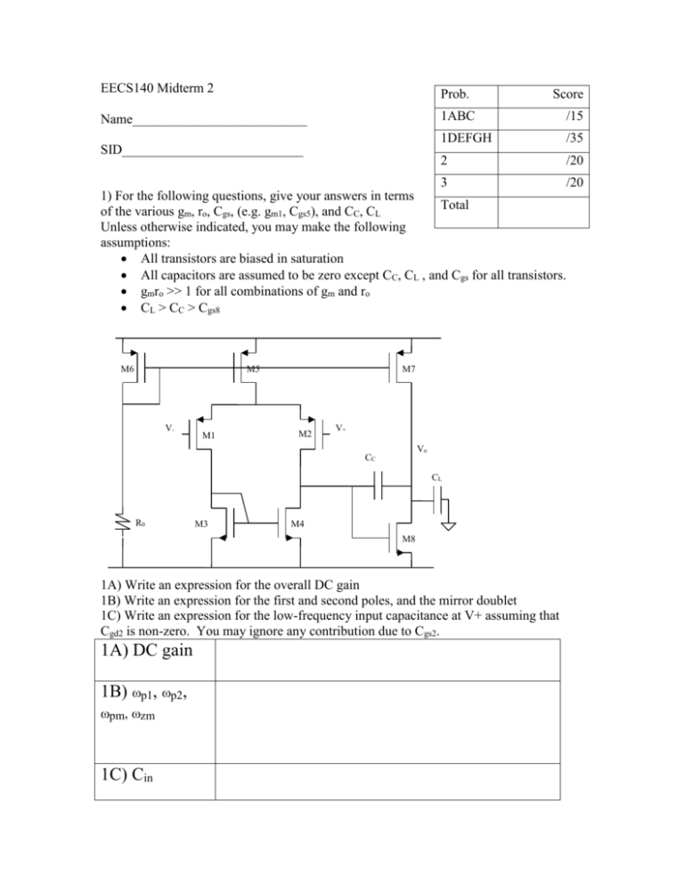
EECS140 Midterm 2 Prob. Name__________________________ 1ABC /15 1DEFGH /35 2 /20 SID___________________________ Score 3 /20 1) For the following questions, give your answers in terms Total of the various gm, ro, Cgs, (e.g. gm1, Cgs5), and CC, CL Unless otherwise indicated, you may make the following assumptions: All transistors are biased in saturation All capacitors are assumed to be zero except CC, CL , and Cgs for all transistors. gmro >> 1 for all combinations of gm and ro CL > CC > Cgs8 M6 M5 V- M1 M7 M2 V+ Vo CC CL R0 M3 M4 M8 1A) Write an expression for the overall DC gain 1B) Write an expression for the first and second poles, and the mirror doublet 1C) Write an expression for the low-frequency input capacitance at V+ assuming that Cgd2 is non-zero. You may ignore any contribution due to Cgs2. 1A) DC gain 1B) p1, p2, pm, zm 1C) Cin Prob. 1, cont.) Assume that the mirror doublet is at very high frequency (well above 10Grad/sec), and the following component values: gm1,2 ro1-6 gm8 ro7,8 CL CC Cgs8 1mS 200k 10mS 2k 10p 1p 0.1p On the following pages, 1D) plot the magnitude of the second stage gain 1E) plot the overall impedance seen at the first stage output (including Ro1, Cgs8, CC, and any effects of Miller multiplication), 1F) plot the magnitude of the first stage gain, 1G) plot the magnitude and phase of the overall gain. Label poles and zeros clearly. 1H) what value of CC is needed for a 45 degree phase margin? 1H) CC 1D) Second stage gain – |Av2,0| 10,000 |Av2,0| |Av2,0| 100 1 1 1k 1M 1G 1E) Impedance at first stage output, |Zo1| 10M |Zo1| |Zo1| 100K 1K 1 1k 1M 1G 1F) First stage gain, |Av1| 10,000 |Av1| |Av1| 100 1 1 1k 1M 1G 1G) op amp Bode plot |Av| 10,000 |Av| 100 1 1 1k 1M 1G 0 Phase(Av) Phase(Av) -90 -180 -270 1 1k 1M 1G For the following questions, give a short answer and justification (2 sentences max). 2A) You need to design an amplifier which will be used in unity-gain feedback. Input signals with an amplitude of up to 10V and frequencies from 20Hz to 20kHz must be reproduced with less than 1mV of error. What is the minimum gain and minimum unitygain frequency of your open-loop amplifier? 2B) Your friend from Stanford tells you that your 2-stage solution to project 1 was stupid, and that you should have used a telescopic cascode. What do you tell him? 2C) Another friend from Stanford tells you that you can improve the phase margin of your amplifier by decreasing the source impedance that is driving it. What do you tell her? 2D) Do we measure phase margin with an open loop or closed loop amplifier? Why? 3)For the current mirror below, assume that all transistors are identical, with Vt=0.5V, and Iref is chosen such that Vdsat1 is 0.3V. 3A) What is the range of values of VBN such that all transistors remain in saturation if Vout=1V? 3B) Assuming you choose a value for VBN which lies in this range, what is the minimum value for Vout such that all transistors are in saturation? (in terms of VBN) 3C) Assume that this circuit is used as a current mirror in a differential amplifier, and that gm/Cgs for all devices is equal, except M2 which due to layout error has 10 times more capacitance between gate and source as the other devices. What effect does the (defective) mirror have on the frequency response of the amplifier (Pole? Poles? Zero? Zeros?). Be precise. 3D) Using another current source of magnitude Iref, one or more FETs, and no other components, design a circuit to set VBN=Vt+3Vdsat1 . 3A) VBN range 3B) min Vout 3C) Freq. Response of differential amplifier w/ bad mirror Draw your solution for part D here. Label all W/L values! Iref Vout Iref M4 VBN M2 M3 Problem 3 & 4 M1
