A20-doc - University of California, Berkeley
advertisement

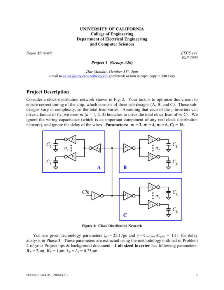
UNIVERSITY OF CALIFORNIA College of Engineering Department of Electrical Engineering and Computer Sciences Dejan Markovic EECS 141 Fall 2005 Project 1 (Group A20) Due Monday, October 31st, 5pm e-mail to ee141@cory.eecs.berkeley.edu (preferred) or turn in paper copy in 240 Cory Project Description Consider a clock distribution network shown in Fig. 2. Your task is to optimize this circuit to ensure correct timing of the chip, which consists of three sub-designs (A, B, and C). These subdesigns vary in complexity, so the total load varies. Assuming that each of the y inverters can drive a fanout of CL, we need nk (k = 1, 2, 3) branches to drive the total clock load of nk·CL. We ignore the wiring capacitance (which is an important component of any real clock distribution network), and ignore the delay of the wires. Parameters: n1 = 2, n2 = 4, n3 = 6, CL = 16. y2 y1 CL x1 n1 x2 n2 CL y2 y1 CL A CL B y3 Clk 1 x3 n3 CL y3 C CL Figure 2: Clock Distribution Network You are given technology parameters tp0 = 25.17ps and = Cintrinsic/Cgate = 1.11 for delay analysis in Phase-3. These parameters are extracted using the methodology outlined in Problem 2 of your Project tips & background document. Unit sized inverter has following parameters: Wp = 2m, Wn = 1m, Lp = Ln = 0.25m. EECS141: FALL 05—PROJECT 1 1 Phase 1: Baseline Design (1/2 week) Determine the sizes xk 1 and yk 1 (k = 1, 2, 3) of the clock inverters to achieve minimum worst-case propagation delay from Clk to all the clock sinks. Propagation delay from Clk to the final clock load is often times referred to as the insertion delay. What is the value of Dmin normalized to tp0? This will be your reference delay for Phase-2. What is the energy Eref dissipated from power supply during a full 010 switching cycle? Express the energy symbolically in terms of Cgate of the unit sized inverter (label Cgate = C to keep it simple) and supply voltage VDD. Now, you have obtained reference point (Dmin, Eref) for your optimizations. Phase 2: Optimized Design (1 week) Now, assume that you are allowed to tolerate slight mismatch in insertion delays. New target insertion delays for the three sub-designs are Dmin, 1.1Dmin, 1.2Dmin. The first goal is to assign these delays to blocks A, B, and C with energy minimization in mind and then perform re-sizing of the gates to minimize energy dissipated by the clock tree. a) What is the optimal assignment of Dmin, 1.1Dmin, 1.2Dmin to A, B, and C? b) What are the optimal sizing factors xk 1 and yk 1 (k = 1, 2, 3)? c) Calculate percent energy reduction compared to the reference energy Eref . Phase 3: Verification in HSPICE (1/2 week) Verify your results from previous two phases in HSPICE. a) Obtain reference point (Dmin, Eref) in HSPICE. Is it different from what you expected? (Hint: CD and CE from Background Problem 1 could help, but this is not the only reason!) b) Using gate size parameters from Phase-2, report simulated delay increase and energy reduction. Determine these numbers relative to the reference case (Dmin, Eref) obtained by HSPICE in part (a) of Phase-3. Comment your results. Report Please use the report template provided at the web-site. Be sure to justify important design decisions and emphasize all the vital information. Organization, conciseness, and completeness are of paramount importance. Make sure to fill out the cover-page and use the correct units. Grading For each phase, the grade will be divided as follows: 30% result 30% correctness 40% approach and report EECS141: FALL 05—PROJECT 1 2


