Solution to Problem 1:
advertisement
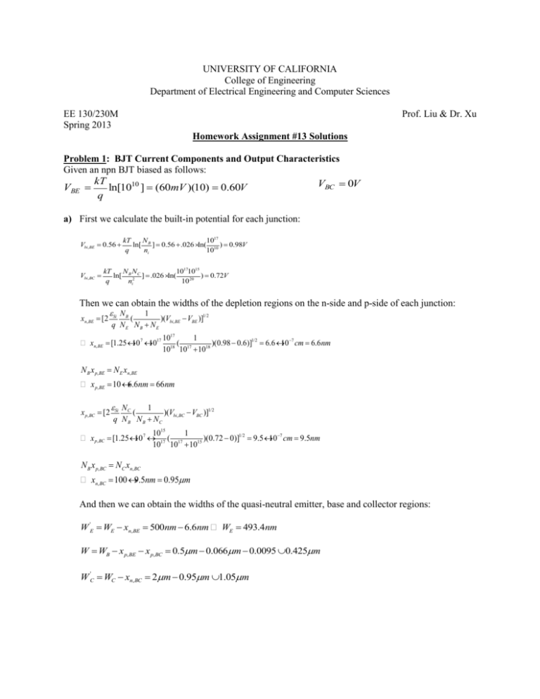
UNIVERSITY OF CALIFORNIA College of Engineering Department of Electrical Engineering and Computer Sciences EE 130/230M Spring 2013 Prof. Liu & Dr. Xu Homework Assignment #13 Solutions Problem 1: BJT Current Components and Output Characteristics Given an npn BJT biased as follows: kT VBC 0V VBE ln[1010 ] (60mV )(10) 0.60V q a) First we calculate the built-in potential for each junction: Vbi,BE = 0.56 + Vbi,BC = kT N 1017 ln[ B ] = 0.56 +.026 × ln( 10 ) = 0.98V q ni 10 kT N N 10171015 ln[ B 2 C ] = .026 × ln( ) = 0.72V q ni 10 20 Then we can obtain the widths of the depletion regions on the n-side and p-side of each junction: xn,BE = [2 eSi N B 1 ( )(Vbi,BE -VBE )]1/2 q NE NB + NE Þ xn,BE = [1.25´10 7 ´1017 1017 1 ( )(0.98 - 0.6)]1/2 = 6.6 ´10-7 cm = 6.6nm 1018 1017 +1018 N B x p,BE = N E xn,BE Þ x p,BE =10 ´ 6.6nm = 66nm x p,BC = [2 eSi NC 1 ( )(Vbi,BC -VBC )]1/2 q N B N B + NC Þ x p,BC = [1.25´10 7 ´ 1015 1 ( )(0.72 - 0)]1/2 = 9.5´10 -7 cm = 9.5nm 1017 1017 +1015 N B x p,BC = NC xn,BC Þ xn,BC =100 ´ 9.5nm = 0.95m m And then we can obtain the widths of the quasi-neutral emitter, base and collector regions: W 'E = WE - xn,BE = 500nm - 6.6nm Þ WE = 493.4nm W = WB - x p,BE - x p,BC = 0.5mm - 0.066mm - 0.0095 » 0.425mm W 'C = WC - xn,BC = 2mm - 0.95mm » 1.05mm We need to determine the minority-carrier diffusivity and diffusion length for each of the quasineutral regions of the BJT, in order to calculate the various current components: From Lecture 4 Slide 15: m E = 150cm 2 / V × s Þ DE = m E Þ LE = kT = 150 cm 2 V -1 s -1 × 0.026V = 3.9 cm 2 / s q DE t E = 3.9 ×10 -7 cm 2 = 6.24 ´10 -4 cm = 6.25m m m B = 770cm 2 / V × s Þ DB = m B Þ LB = kT = 770 cm 2 V -1 s -1 × 0.026V = 20.02 cm 2 / s q DBt B = 20.02 ×10 -6 cm 2 = 4.47 ´10 -3 cm = 44.7m m Note that the minority carrier diffusion length LB is significantly longer than the quasi-neutral base width W (by a factor >100×). mC = 480cm 2 / V × s Þ DC = mC Þ LC = kT = 480 cm 2 V -1 s -1 ´ 0.026V = 12.48cm 2 / s q DCt C = 12.48 ´10 -5 cm 2 = 0.0117cm = 117m m Note that the minority carrier diffusion length LC is significantly longer than the quasi-neutral collector width W’c (by a factor >100×). The excess minority-carrier concentrations at the edges of the depletion regions are nB0 (eqVBE /kT -1) @ 10 20 10 10 = 1013 cm-3 1017 pE 0 (e qVBE / kT 1) pC 0 (e qVBC / kT 1) 1020 10 10 1012 cm 3 1018 10 20 0 (e 1) 0cm 3 15 10 I Ep qA DE cosh(WE ' / LE ) qVBE / kT pE 0 e 1 LE sinh( WE ' / LE ) Þ I Ep = 1.6 ´10-19 C(10 -7 cm 2 ) -4 -4 3.9cm 2 / s 2 -3 cosh(0.494 ´10 cm / 6.25´10 cm) 10 cm 1010 -1) ( -4 -4 -4 6.25´10 cm sinh(0.494 ´10 cm / 6.25 ´10 cm) Þ I Ep = 1.6 ´10-19 C(10 -7 cm 2 ) 3.9cm 2 / s 10 2 cm-3 ´12.68 ´ (1010 -1) -4 6.25´10 cm Þ I Ep = 1.26 ´10-9 A I En = qA DB cosh(W /L nB 0 éë sinh(W /LBB)) (e qVBE /kT -1) - sinh(W1 /LB ) eqVBC /kT -1 ùû LB ( ) for W<<L B, cosh(W/L B )≈1 and sinh(W/L B )≈W/L B D Þ I En = qA B nB 0 éë(e qVBE /kT -1) - eqVBC /kT -1 ùû W 20.02 Þ I En = 1.6 ´10 -19 ´10 -7 ´ ´10 4 ´ éë(1010 -1) - (1-1)ùû -4 0.425 ´10 -7 Þ I En = 7.5 ´10 A ( I Cp qA ) DC cosh(WC ' / LC ) qVBC / kT pC 0 (e 1) LC sinh( WC ' / LC ) I Cp qA DC cosh(WC ' / LC ) 0 (0) (e 1) LC sinh(WC ' / LC ) I Cp 0 A I Cn qA DB nB 0 LB 1 sinh(W / LB ) ( e qVBE / kT 1) sinh(W / LBB)) e qVBC / kT 1 cosh(W / L for W << L B , cosh(W/L B ) ≈1 and sinh(W/L B ) ≈ W/L B I Cn I Cn DB n B 0 ( e qVBE / kT 1) e qVBC / kT 1 W 20.02 1.6 10 19 10 7 104 (1010 1) 1 1 0.425 10 4 7.5 10 7 A I Cn qA The BJT terminal currents are: I E = I En + I Ep = 750nA +1.26nA = 751.26nA IC = ICn + ICp = 750nA + 0A = 750nA I B = I E - IC = 1.26nA The performance parameters are: gº I En » 0.998 I En + I Ep aT º I Cn »1 I En bdc º IC » 595.2 IB b) The output characteristic (IC vs. VCE) for 0 < VCE < 3 V is sketched below. At VCE = 3.0 V, VCB = 2.4 V since VBE is fixed at 0.6 V. In this operating condition, x p , BC [2 Si N C 1 ( )(Vbi, BC V BC )]1 / 2 q N B N B NC 10 12 1015 1 ( )( 0.72 2.4)]1 / 2 1.6 10 19 1017 1015 1017 1.97 10 6 cm 0.0197 m x p , BC [2 x p , BC W WB x p ,BE x p ,BC 0.5m 0.066m 0.0197 0.414 m The quasi-neutral base width W changes by only ~2% when VCE is swept from 0.6 to 3V. Thus base width modulation is not significant for this BJT. c) IB is proportional to the factor eqVBE /kT . For doubling IB, eqVBE /kT = 2 ´1010 Þ VBE = 0.617V Since VBE would only need to change slightly to double IB, there would be negligible change in xp,BE. Therefore the values of the performance parameters calculated in part (a) would not change significantly. As shown in the plot above, doubling the value of IB in part doubles the value of IC. Problem 2: Ebers-Moll Model Note that the “diode” current I is the BJT emitter current IE. From the Ebers-Moll equation for IE, I I E I F 0 (e qVEB / kT 1) R I R 0 (e qVCB / kT 1) (Equation 1) However, we need to express I as a function of VA, rather than VEB and VCB, i.e. I should be expressed as a function of (e qVA / kT 1) . 1) and (e 1) so that we can “simplify” First, let’s find a relationship between (e Equation 1. We can do this by noting that IB = 0 so that IE = IC. Equating the Ebers-Moll expressions for IE and IC: qVEB / kT qVCB / kT I F 0 (e qVEB / kT 1) R I R 0 (e qVCB / kT 1) F I F 0 (e qVEB / kT 1) I R 0 (e qVCB / kT 1) (1 F ) I F 0 (e qVEB / kT 1) (1 R ) I R 0 (e qVCB / kT 1) (e qVEB / kT 1) (e qVCB / kT 1) 1 R I R 0 where 1 F I F 0 Therefore (Equation 2) Next, let’s find a relationship between VCB and VA: VA VEC VEB VBC VEB VCB VEB VA VCB so eqVEB / kT 1 eqVA / kT eVCB / kT 1 eqVA / kT (eqVCB / kT 1) (eqVA / kT 1) Eliminating VEB in the above equation by applying Equation 2, and then combining terms, we obtain (e qVA / kT )(e qVCB / kT 1) (e qVA / kT 1) (e qVCB / kT (e qVA / kT 1) 1) qVA / kT (e ) (e qVEB / kT 1) (e (e qV (Equation 3) 1) ) qVA / kT A / kT (Equation 4) Applying Equations 3 and 4 to Equation 1, and rearranging terms, we obtain (1 R F ) I R 0 I F 0 (e qVA / kT 1) I (1 F ) I F 0e qVA / kT (1 R ) I R 0 Note that in this configuration, the BJT does not exhibit ordinary diode-like characteristics: Under “forward bias” with VA greater than several kT/q, the second term in the denominator is small relative to the first term in the denominator, so that I (1 R F ) I R 0 I R0 (1 F ) Thus, the forward “diode” current is essentially the reverse-bias current of the collector pnjunction. For large “reverse bias” with |VA| larger than several kT/q, I (1 R F ) I F 0 I F 0 (1 R ) Thus, the reverse “diode” current is essentially the reverse-bias current of the emitter pnjunction. Therefore, very little current flows in either direction for a BJT connected in this configuration. Problem 3: BJT – Deviations from the Ideal a) The Early voltage (VA) is given by the following equation: VA qN BW C JC where CJC has units of Farads per cm2: CJC = eSi Wdep,BC = eSi x p,BC + xn,BC = (10-12 F / cm) = 1.04 ´10-8 F / cm 2 (9.5 + 950) ´10-7 cm Thus, VA = (1.6 ´10 -19 C)(1017 cm-3 )(0.425 ´10-4 cm) = 65.38V 1.04 ´10 -8 F / cm 2 b) For an npn BJT, we arrive at the following equation for VBC at punchthrough: For a step junction, é 2e ù NC x 2p,BC = ê si (Vbi,BC - VBC )ú ë q N B (N C + N B ) û The width of the base that is not depleted, W = WB - x p,BE - x p,BC At punchthrough, W = 0 Þ x 2p,BC = (WB - x p,BE )2 Þ VBC = Vbi,BC - (WB - x p,BE )2 2e si NC ( ) q N B (N C + N B ) Þ VBC = 0.72V - (0.425 ´10 -4 cm - 0.065 ´10-4 cm)2 2 ´1.0 ´10-12 F / cm 1015 cm-3 ( ) 1.6 ´10-19 C 1017 cm-3 (1´1017 cm-3 ) Þ VBC = 0.72 -1036.8 @ -1036V Therefore, VPT º VCE,PT = VCB +VBE =1036V + 0.6V @1036V c) The breakdown voltage (VCE0) is determined as follows: First, calculate the reverse breakdown voltage of the base-collector junction (VCB0), considering that it breaks down when the peak electric field max qN B Si VCB 0 Þ VCB 0 = x p , BC [ 2 q Si Si ( NC N B ) 2qNC N B ( max=5105 V/cm: NC N B )(Vbi , BC VCB 0 )]1 / 2 NC N B ( max ) 2 Vbi , BC 10-12 F / cm(1.0 ´1017 cm-3 ) (5×10 5 V / cm)2 - 0.72V 2 ´1.6 ´10-19 C ´1015 cm-3 ´1017 cm-3 Þ VCB0 » 780.5V Therefore, VCE 0 = VCB0 bdc +1 = 780.5V » 98.3V 62 +1 d) Comparing the answers obtained in parts (b) and (c), we see that the punchthrough voltage (VPT) is larger (in magnitude) than the (common-emitter) breakdown voltage (VCE0). Therefore, punchthrough will not occur before breakdown in the common-emitter output characteristics of this BJT. Problem 4: Gummel Plot If we assume an npn BJT: a) If NB is increased, IEn (the injected electron current from the emitter to the base) decreases, n 2i DB . This will result in a decrease in Ic by the same factor. I En N B WB b) As NE is increased, IEp (the injected hole current from the base to the emitter) decreases, n 2i DE . If recombination in the quasi-neutral base is negligible, then IB is dominated I Ep N E WE by carrier injection to the emitter and will decrease by the same factor. c) If the base width decreases by a factor of 2, the excess carrier concentration goes to zero (at the edge of the collector junction depletion region) within half the distance, i.e. the carrier concentration gradient becomes twice as steep so Ic doubles. d) As temperature increases, ni also increases (recall that ni is exponentially dependent on 2 temperature). Therefore the currents IB and IC also increase ( I » ni eqV kT ). Moreover, the N slope of the diffusion current is proportional to 1/(kT/q), hence we should also expect a decrease in the slope of the log(I) vs. VBE curve. The Gummel plots corresponding to (a), (b), (c) and (d) are drawn below. (The black curves correspond to a reference BJT design, while the colored curves show the impact of the changes.)
