SEM, AFM, STM: Nanoscience & Microscopy Techniques
advertisement
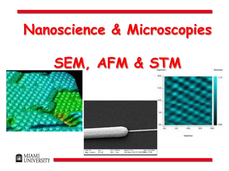
Nanoscience & Microscopies SEM, AFM & STM Block Diagram of E-beam SEM Picts SEM Picts Dendritic Growth Ostrinium Nubilialis Miami Research Results STM • Scanning tunneling microscope Outside the Barrier Wavefunction extends outside of well edge for a finite square well Two finite wells at a distance • The electron wavefunctions extend into space between finite wells http://www.chembio.uoguelph.ca/educmat/chm729/STMpage/stmdet.htm Two finite wells at close approach can look like a barrier to the electrons! • Electrons can tunnel into or through barriers depending on… http://phys.educ.ksu.edu/vqm/html/qtunneling.html Two finite wells at close approach • Electron wavefunctions can overlap http://www.chembio.uoguelph.ca/educmat/chm729/STMpage/stmdet.htm • This is the STM image of Si(111)-7x7 surface, the white spots represents the position of the atoms. Scanning -• Constant Current Mode • Constant Height Mode • http://www.surfaces.lsu.edu/ST Moverview.html www.surfaces.lsu.edu/STMoverview.html Modes of Operation • Constant Current • Constant Height userpage.chemie.fu-berlin.de/.../html/node5.htm Use of STM- Chemical Constrast The surface of alloys may differ in several respects from the corresponding bulk structure. The surface may also exhibit a chemical order different from the one in the bulk of the material. This influences processes such as gas adsorption and catalysis, since adsorbed molecules often prefer a certain chemical environment of substrate atoms. It all started with an (111) oriented surface of a PtNi alloy (bulk composition 25% Pt, 75% Ni; surface approx. 50% of each). We found that we can distinguish between Pt and Ni atoms on this surface with the STM! Since Pt and Ni are about 50% of the surface atoms each, the brighter species is Ni. The white blobs in the image are impurities of unknown nature. http://www.iap.tuwien.ac.at/www/surface/STM_Gallery/chemical_resolution.html Use of STM • Excitation of different vibrational modes depending on species (C2H2 vs. C2D2) – Science, 280, 1715 (1998). • Single molecule chemical reactions – Science News, 158, 215 (2000). Researchers usually compare "before" and "after" pictures of typical regions of a material to see how it changes during a phase transition. This is now see on an atomic scale. As the lead atoms in this 20 x 13 nanometer region are warmed from 40 to 136 Kelvin, they switch from the corrugated to the flat arrangement at the transition temperature of 86 Kelvin . Vienna University of Technology Phys. Rev. Lett. 94, 046101 Downside to STM? • Requires electrical path – for tunneling • Gives information of heights of electron clouds above surface – eg. graphite structure • Some questions cannot be explored Other cool sites… • http://www.almaden.ibm.com/vis/stm (Interesting STM images) • http://www.nobel.se/physics/educational/ microscopes/scanning/ (Interesting STM images) Atomic Force Microscopy AFM • Cantilever structure on end on end of wafer holds the pyramidal tip • Light from a diode laser bounces of tip and strikes a split photodetector • Motion is detected by differences in intensity on the detector portions http://www.stolaf.edu/depts/physics/afm/diagram.html Let’s also look at: http://www.weizmann.ac.il/Chemical_Research_Support/surflab/peter/afmworks/ Wafer & TIP • Si or SiN – 10 nm at end – ~100 atoms Electron micrograph of two 100 µm long V-shaped cantilevers (by Jean-Paul Revel, Caltech; cantilevers from Park Scientific Instruments, Sunnyvale, CA). Three common types of AFM tip. (a) normal tip (3 µm tall); (b) supertip; (c) Ultralever (also 3 µm tall). (b) Electron micrographs by Jean-Paul Revel, Caltech. http://stm2.nrl.navy.mil/how-afm/how-afm.html General Schematic AFM Modes • Contact – Low and High Gain • Low gain – “drag” tip across sample see deflection which is OK for relatively flat surfaces • High gain – tries to push down on sample to maintain a particular height which is OK for more bumpy surfaces, but not for soft surfaces - Tapping mode • Good for local surface distortions to measure friction and spring forces on surfaces • Non-contact – Requires a frequency modulation technique which is good for biological samples- repulsive forces from surface Metrology -- Fabrication • AFM can be used to study the success of e-beam lithography and subsequent processing steps. Nanotechnology, 13 659 (2002). AFM – DNA studies Results Tobacco Mosaic Virus Non-Contact Mode – Solid Lipid Nanoparticles STM & AFM • Microscopic techniques which give us resolutions in angstroms or nanometers • Used for fabrication, chemical and biological studies • A definite “force” in the nanoworld !
