Photoluminescence-Excitation Mapping of Single Walled Carbon
advertisement
Photoluminescence-Excitation Mapping of
Single Walled Carbon Nanotubes
Adrian Nish, Robin J Nicholas
Department of Physics, Clarendon Laboratory, Parks Road, Oxford, OX1 3PU, UK
e-mail: a.nish1@physics.ox.ac.uk
PLE Mapping
Introduction
Photoluminescence-Excitation
mapping
has become one of the most useful
methods for characterising different
samples of SWNTs in terms of their
constituent
semi-conducting
species.
Some of the background, experimental
method and current work on analysing
these spectra is presented here.
Single-Walled Carbon Nanotubes
• The intensity of PL is very sensitive to the wavelength of excitation
• Two systems are currently used for excitation:
-75W Xenon lamp & 0.3m monochromator with a linewidth of <1nm4
{ 300-950nm }
-Tunable Ti:Sapphire
{ 700-990nm }
laser
with
a
linewidth
of
0.05nm
• A Si-CCD {800-1100nm} and InGaAs PDA {900-1600nm} are used for
detection
PLE Map taken with the
system in the above
schematic
• Hexagonal network of carbon atoms rolled up to
make a seamless cylinder
• Different ‘cuts’ have
different helicities as
defined by the ‘chiral
angle‘
• Structure and diameter
are given by integer
values (n,m) from C =
na1 + ma2 where a1 & a2
are lattice unit vectors
and C is circumference
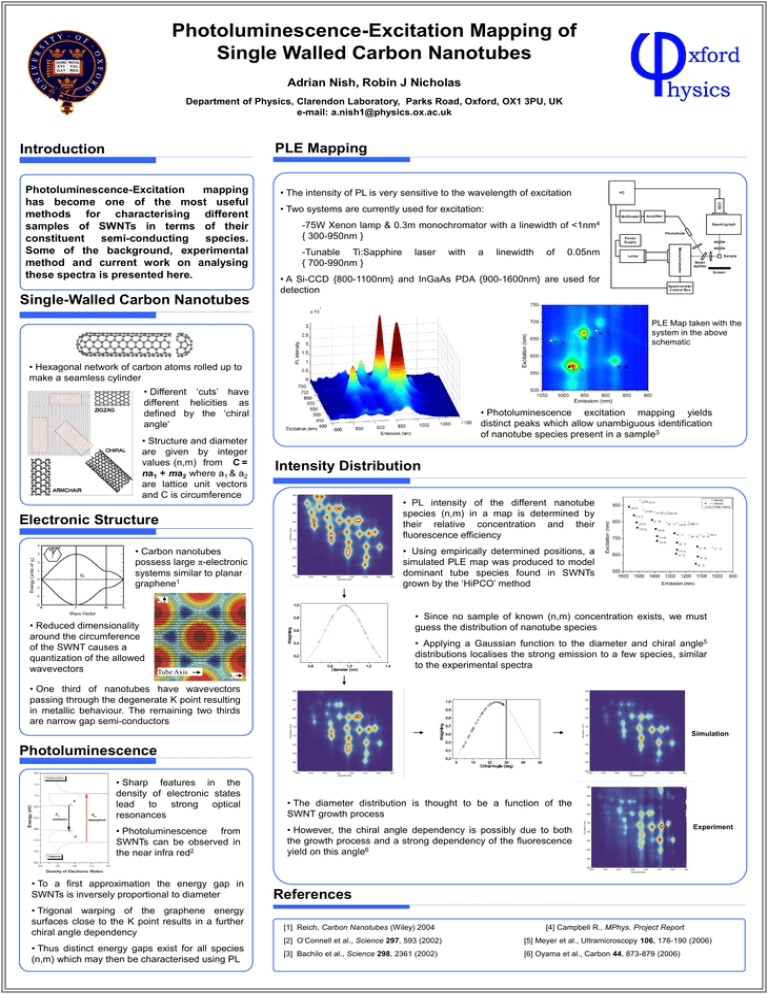
• Photoluminescence excitation mapping yields
distinct peaks which allow unambiguous identification
of nanotube species present in a sample3
Intensity Distribution
• PL intensity of the different nanotube
species (n,m) in a map is determined by
their relative concentration and their
fluorescence efficiency
Electronic Structure
• Using empirically determined positions, a
simulated PLE map was produced to model
dominant tube species found in SWNTs
grown by the ‘HiPCO’ method
• Carbon nanotubes
possess large π-electronic
systems similar to planar
graphene1
kx
• Reduced dimensionality
around the circumference
of the SWNT causes a
quantization of the allowed
wavevectors
• Since no sample of known (n,m) concentration exists, we must
guess the distribution of nanotube species
Tube Axis
• Applying a Gaussian function to the diameter and chiral angle5
distributions localises the strong emission to a few species, similar
to the experimental spectra
ky
• One third of nanotubes have wavevectors
passing through the degenerate K point resulting
in metallic behaviour. The remaining two thirds
are narrow gap semi-conductors
Simulation
Photoluminescence
• Sharp features in the
density of electronic states
lead to strong optical
resonances
• The diameter distribution is thought to be a function of the
SWNT growth process
• Photoluminescence from
SWNTs can be observed in
the near infra red2
• However, the chiral angle dependency is possibly due to both
the growth process and a strong dependency of the fluorescence
yield on this angle6
• To a first approximation the energy gap in
SWNTs is inversely proportional to diameter
• Trigonal warping of the graphene energy
surfaces close to the K point results in a further
chiral angle dependency
• Thus distinct energy gaps exist for all species
(n,m) which may then be characterised using PL
Experiment
References
[1] Reich, Carbon Nanotubes (Wiley) 2004
[4] Campbell R., MPhys. Project Report
[2] O’Connell et al., Science 297, 593 (2002)
[5] Meyer et al., Ultramicroscopy 106, 176-190 (2006)
[3] Bachilo et al., Science 298, 2361 (2002)
[6] Oyama et al., Carbon 44, 873-879 (2006)
