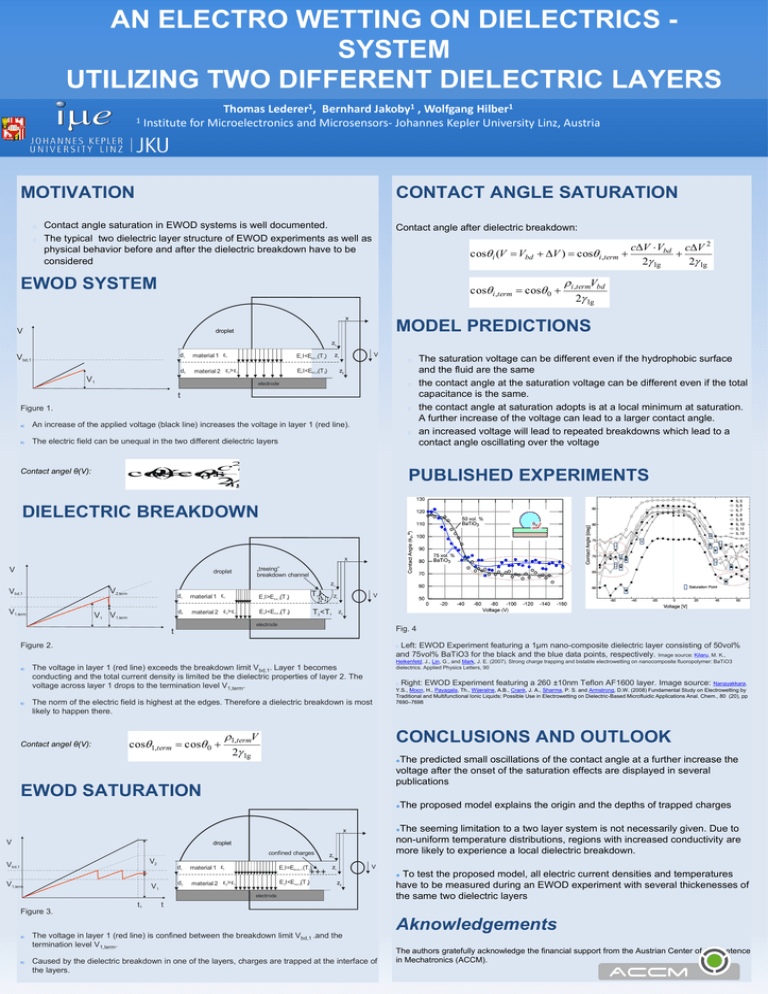
AN ELECTRO WETTING ON DIELECTRICS SYSTEM
UTILIZING TWO DIFFERENT DIELECTRIC LAYERS
Thomas Lederer1, Bernhard Jakoby1 , Wolfgang Hilber1
1 Institute for Microelectronics and Microsensors- Johannes Kepler University Linz, Austria
MOTIVATION
CONTACT ANGLE SATURATION
Contact angle saturation in EWOD systems is well documented.
The typical two dielectric layer structure of EWOD experiments as well as
physical behavior before and after the dielectric breakdown have to be
considered
Contact angle after dielectric breakdown:
cos i (V Vbd
EWOD SYSTEM
cos i ,term
x
V
cV Vbd cV 2
V ) cos i ,term
2 lg
2 lg
i ,termVbd
cos 0
2 lg
MODEL PREDICTIONS
droplet
z1
Vbd,1
d1
material 1 ε1
E1I>Eb d ,1(T 1) E1 I<Eb d ,1(T 1)
d2
material 2 ε2> ε1
E2I<Eb d ,2(T 2) E2 I<Eb d ,2(T 2)
V1
V
zi
The saturation voltage can be different even if the hydrophobic surface
and the fluid are the same
the contact angle at the saturation voltage can be different even if the total
capacitance is the same.
the contact angle at saturation adopts is at a local minimum at saturation.
A further increase of the voltage can lead to a larger contact angle.
an increased voltage will lead to repeated breakdowns which lead to a
contact angle oscillating over the voltage
z2
electrode
t
Figure 1.
a)
An increase of the applied voltage (black line) increases the voltage in layer 1 (red line).
b)
The electric field can be unequal in the two different dielectric layers
Contact angel θ(V):
2
cV
cos
V
cos
0
2
lg
PUBLISHED EXPERIMENTS
DIELECTRIC BREAKDOWN
x
V
droplet
„treeing”
breakdown channel
z1
V2,term
Vbd,1
V1,term
V1 V1,term
d1
material 1 ε1
E1I>Eb d ,1(T 1)
T1
d2
material 2 ε2> ε1
E2I<Eb d ,2(T 2)
T2 <T1
V
zi
z2
electrode
Fig. 4
t
Left: EWOD Experiment featuring a 1µm nano-composite dielectric layer consisting of 50vol%
and 75vol% BaTiO3 for the black and the blue data points, respectively. Image source: Kilaru, M. K.,
Figure 2.
a)
b)
Heikenfeld, J., Lin, G., and Mark, J. E. (2007). Strong charge trapping and bistable electrowetting on nanocomposite fluoropolymer: BaTiO3
dielectrics. Applied Physics Letters, 90
The voltage in layer 1 (red line) exceeds the breakdown limit Vbd,1. Layer 1 becomes
conducting and the total current density is limited be the dielectric properties of layer 2. The
voltage across layer 1 drops to the termination level V1,term.
Right: EWOD Experiment featuring a 260 ±10nm Teflon AF1600 layer. Image source: Nanayakkara,
The norm of the electric field is highest at the edges. Therefore a dielectric breakdown is most
likely to happen there.
Contact angel θ(V):
cos1,term
1,termV
cos 0
2 lg
Y.S., Moon, H., Payagala, Th., Wijeratne, A.B., Crank, J. A., Sharma, P. S. and Armstrong, D.W. (2008) Fundamental Study on Electrowetting by
Traditional and Multifunctional Ionic Liquids: Possible Use in Electrowetting on Dielectric-Based Microfluidic Applications Anal. Chem., 80 (20), pp
7690–7698
CONCLUSIONS AND OUTLOOK
The predicted small oscillations of the contact angle at a further increase the
voltage after the onset of the saturation effects are displayed in several
publications
EWOD SATURATION
The seeming limitation to a two layer system is not necessarily given. Due to
non-uniform temperature distributions, regions with increased conductivity are
more likely to experience a local dielectric breakdown.
x
V
droplet
confined charges
V2
Vbd,1
V1,term
d1
d2
V1
material 1 ε1
material 2 ε2> ε1
E1 I=E
E1I>Eb d ,1(T
) te rm,1 (T1)
1
+++
E2I<E
(T 2)
E2I<Eb d ,2(T
b d ,2
2)
z1
V
zi
Figure 3.
a)
b)
To test the proposed model, all electric current densities and temperatures
have to be measured during an EWOD experiment with several thickenesses of
the same two dielectric layers
z2
electrode
t1
The proposed model explains the origin and the depths of trapped charges
t
The voltage in layer 1 (red line) is confined between the breakdown limit Vbd,1 .and the
termination level V1,term.
Caused by the dielectric breakdown in one of the layers, charges are trapped at the interface of
the layers.
Aknowledgements
The authors gratefully acknowledge the financial support from the Austrian Center of Competence
in Mechatronics (ACCM).
