Semiconductor Equilibrium: Charge Carriers & Doping
advertisement
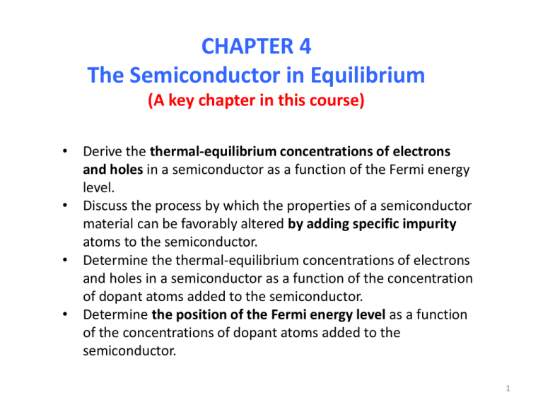
CHAPTER 4 The Semiconductor in Equilibrium (A key chapter in this course) • Derive the thermal-equilibrium concentrations of electrons and holes in a semiconductor as a function of the Fermi energy level. • Discuss the process by which the properties of a semiconductor material can be favorably altered by adding specific impurity atoms to the semiconductor. • Determine the thermal-equilibrium concentrations of electrons and holes in a semiconductor as a function of the concentration of dopant atoms added to the semiconductor. • Determine the position of the Fermi energy level as a function of the concentrations of dopant atoms added to the semiconductor. 1 4.1 | CHARGE CARRIERS IN SEMICONDUCTORS 4.1.1 Equilibrium Distribution of Electrons and Holes • a plot of the density of states function in the conduction-band gc(E), the density of states function in the valence-band gv(E), and the Fermi–Dirac probability function for T > 0 K when EF is approximately halfway between Ec and Ev. • Assume that the electron and hole effective masses are equal, then gc(E) and gv(E) are symmetrical functions about the midgap energy. • Note that the function fF (E ) for E > EF is symmetrical to the function 1 - fF (E) for E < EF about the energy E = EF. 2 3 4.1.2 The n0 and p0 Equations Thermal-Equilibrium Electron Concentration 4 Comment of Example 4.1: The probability of a state being occupied can be quite small, but the fact that there are a large number of states means that the electron concentration is a reasonable value. 5 Comment of Ex 4.2: The parameter values at any temperature can easily be found by using the 300 K values and the temperature dependence. Note that the value of Nc for gallium arsenide is smaller than the typical 1019 cm-3 value due to the small electron effective mass in gallium arsenide. 6 • Comment of Ex 4.3: the intrinsic carrier concentration increased by over 4 orders of magnitude as the temperature increased by 150°C. • the value of ni for these semiconductors may easily vary over several orders of magnitude as the temperature changes over a reasonable range. 7 4.1.4 The Intrinsic Fermi-Level Position The intrinsic Fermi level must shift away from the band with the larger density of states in order to maintain equal numbers of electrons and 8 Comment of Ex 4.4, The intrinsic Fermi level in silicon is 12.8 meV below the midgap energy. If we compare 12.8 meV to 560 meV, which is one-half of the bandgap energy of silicon, we can, in many applications, simply approximate the intrinsic Fermi level to be in the center of the bandgap. 4.2 | DOPANT ATOMS AND ENERGY LEVELS The doped semiconductor, called an extrinsic material • The phosphorus atom without the donor electron is positively charged. 9 This type of impurity atom donates an electron to the conduction band and so is called a donor impurity atom. The group III atom accepts an electron from the valence band and so is referred to as an acceptor impurity atom. 10 4.2.2 Ionization Energy ionization energy: the approximate energy required to elevate the donor electron into the conduction band. The donor electron is not tightly bound to the donor atom. 11 For silicon, the ionization energy is E = -25.8 meV, much less than the bandgap energy . 12 4.2.3 Group III–V Semiconductors • Group IV elements, such as silicon and germanium, can also be impurity atoms in gallium arsenide. Such impurities are called amphoteric • germanium is predominantly an acceptor and silicon is predominantly a donor. 4.3 | THE EXTRINSIC SEMICONDUCTOR An extrinsic semiconductor is defined as a semiconductor in which controlled amounts of specific dopant or impurity atoms have been added so that the thermal-equilibrium electron and hole concentrations are different from the intrinsic carrier concentration. 13 14 Comment of Ex 4.5 • The change in the Fermi level is actually a function of the donor or acceptor impurity concentrations that are added to the semiconductor. • electron and hole concentrations change by orders of magnitude from the intrinsic carrier concentration as the Fermi energy changes by a few tenths of an electron-volt. 4.3.2 The n0 p0 Product 15 When Ef is near or over Ec, the Boltzmann approximation is not valid. 16 4.3.4 Degenerate and Nondegenerate Semiconductors • As the donor concentration further increases, the band of donor states widens and may overlap the bottom of the conduction band. • This overlap occurs when the donor concentration becomes comparable with the effective density of states. • When the concentration of electrons in the conduction band exceeds the density of states Nc, the Fermi energy lies within the conduction band. This type of semiconductor is called a degenerate n-type semiconductor. • In the degenerate n-type semiconductor, the states between EF and Ec are mostly filled with electrons; thus, the electron concentration in the conduction band is very large. 17 4.4 | STATISTICS OF DONORS AND ACCEPTORS 4.4.1 Probability Function where nd is the density of electrons occupying the donor level and Ed is the energy of the donor level. The factor 1/2 in this equation is a direct result of the spin factor just mentioned. 4.4.2 Complete Ionization and Freeze-Out 18 Comment Ex 4.7 there are very few electrons in the donor state compared with the conduction band. Essentially all of the electrons from the donor states are in the conduction band and, since only about 0.4 percent of the donor states contain electrons, the donor states are said to be completely ionized. 19 at T = 0 K, No electrons from the donor state are thermally elevated into the conduction band; this effect is called freeze-out. Similarly, when no electrons from the valance band are elevated into the acceptor states, the effect is also called freeze-out. Comment Ex 4.8, at approximately 100C below room temperature, we still have 90 percent of the acceptor atoms ionized; in other words, 90 percent of the acceptor atoms have “donated” a hole to the valence band. 20 4.5 | CHARGE NEUTRALITY 4.5.1 Compensated Semiconductors A compensated semiconductor is one that contains both donor and acceptor impurity atoms in the same region. 4.5.2 Equilibrium Electron and Hole Concentrations The charge neutrality condition is expressed by equating the density of negative charges to the density of positive charges. 21 Comment ex 4.9, (Nd - Na) > ni, so the thermal-equilibrium majority carrier electron concentration is essentially equal to the difference between the donor and acceptor concentrations. the majority carrier electron concentration is orders of magnitude larger than the minority carrier hole concentration. 22 A few of the donor electrons will fall into the empty states in the valence band and, in doing so, will annihilate some of the intrinsic holes. Comment Ex 4.10, If the donor impurity concentration is not too different in magnitude from the intrinsic carrier concentration, then the thermal-equilibrium majority carrier electron concentration is influenced by the intrinsic concentration. 23 Silicon doped with 5 X 10¹⁴ donors As the temperature increases, we can see where the intrinsic concentration begins to dominate. Also shown is the partial ionization, or the onset of freeze-out, at the low temperature. 24 Comment Ex. 4.11, If we assume complete ionization and if (Na - Nd) > ni, then the majority carrier hole concentration is, to a very good approximation, just the difference between the acceptor and donor concentrations. 4.6 | POSITION OF FERMI ENERGY LEVEL 4.6.1 Mathematical Derivation 25 26 4.6.2 Variation of EF with Doping Concentration and Temperature Comment Ex 4.13 If the acceptor (or donor) concentration in silicon is greater than approximately 3 X 1017 cm-3, then the Boltzmann approximation of the distribution function becomes less valid and the equations for the Fermi-level position are no longer quite as accurate. 27 At the low temperature where freeze-out occurs, the Fermi level goes above Ed for the n-type material and below Ea for the p-type material. 28 in thermal equilibrium, the Fermi energy level is a constant throughout a system. 29

