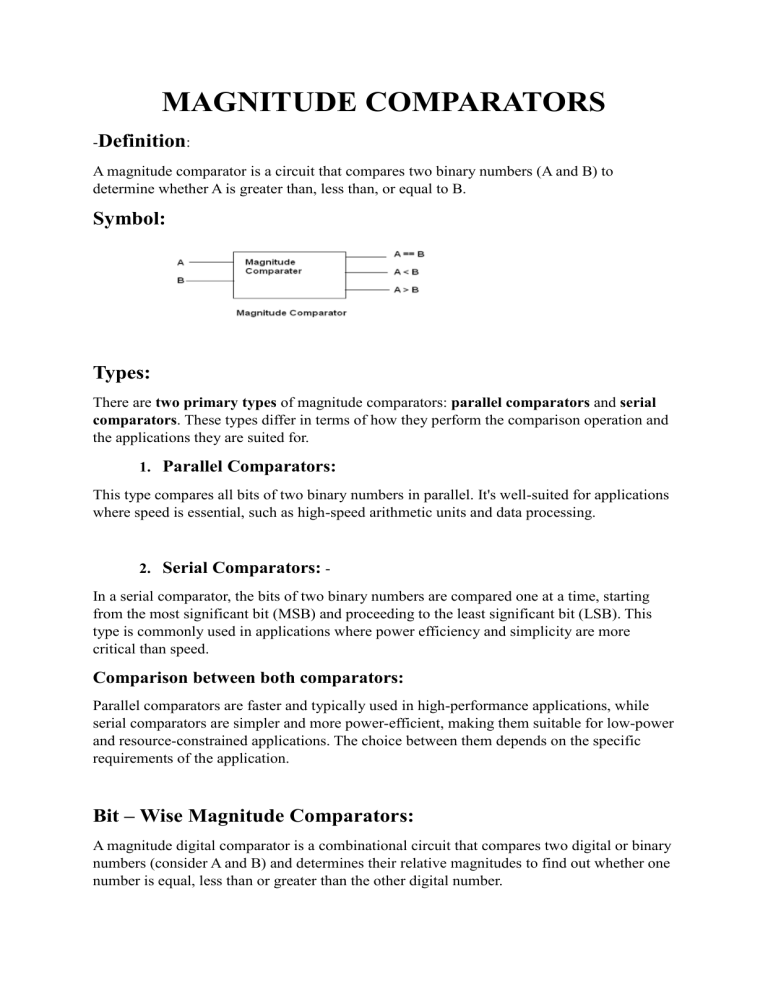
MAGNITUDE COMPARATORS -Definition: A magnitude comparator is a circuit that compares two binary numbers (A and B) to determine whether A is greater than, less than, or equal to B. Symbol: Types: There are two primary types of magnitude comparators: parallel comparators and serial comparators. These types differ in terms of how they perform the comparison operation and the applications they are suited for. 1. Parallel Comparators: This type compares all bits of two binary numbers in parallel. It's well-suited for applications where speed is essential, such as high-speed arithmetic units and data processing. 2. Serial Comparators: In a serial comparator, the bits of two binary numbers are compared one at a time, starting from the most significant bit (MSB) and proceeding to the least significant bit (LSB). This type is commonly used in applications where power efficiency and simplicity are more critical than speed. Comparison between both comparators: Parallel comparators are faster and typically used in high-performance applications, while serial comparators are simpler and more power-efficient, making them suitable for low-power and resource-constrained applications. The choice between them depends on the specific requirements of the application. Bit – Wise Magnitude Comparators: A magnitude digital comparator is a combinational circuit that compares two digital or binary numbers (consider A and B) and determines their relative magnitudes to find out whether one number is equal, less than or greater than the other digital number. Three binary variables are used to indicate the outcome of the comparison as A>B, A<B, or A=B. The below figure shows the block diagram of a n-bit comparator which compares the two numbers of n-bit length and generates their relation between themselves. ICs of Different Bit-Wise Comparators: These comparators can compare 2-bit, 4-bit depending on the application requirement. These are available in TTL as well as CMOS logic family ICs and some of these ICs include IC 7485 (4-bit comparator), IC 4585 (4-bit comparator in CMOS family) Single Bit Magnitude Comparator A comparator used to compare two bits, i.e., two numbers each of single bit is called a single bit comparator. It consists of two inputs for allowing two single bit numbers and three outputs to generate less than, equal and greater than comparison outputs. The figure below shows the block diagram of a single bit magnitude comparator. This comparator compares the two bits and produces one of the 3 outputs as L (A<B), E (A=B) and G (A>B). Circuit Truth Table K-Map: Equation: Logic Circuit Diagram: By using these Boolean expressions, we can implement a logic circuit for this comparator using two AND gates, one NOT gate and one Ex-NOR gate as shown in below figure. AND gates are used to find whether a binary digit is less than greater than another bit whereas ExNOR gate is used to find whether two binary numbers are equal or not. 4-Bit Comparator Circuit: Truth Table: Equation: It compares each of these bits in one number with bits in that of other number and produces one of the following outputs as A = B, A < B and A>B. The output logic statements of this converter are 1. If A3 = 1 and B3 = 0, then A is greater than B (A>B). Or 2. If A3 and B3 are equal, and if A2 = 1 and B2 = 0, then A > B. Or 3. If A3 and B3 are equal & A2 and B2 are equal, and if A1 = 1, and B1 = 0, then A>B. Or 4. If A3 and B3 are equal, A2 and B2 are equal and A1 and B1 are equal, and if A0 = 1 and B0 = 0, then A > B. From the above statements, the output A > B logic expression can be written as The equal output is produced when all the individual bits of one number are exactly coincides with corresponding bits of another number. Then the logical expression for A=B output can be written as E = (A3 Ex-NOR B3) (A2 Ex-NOR B2) (A1 Ex-NOR B1) (A0 Ex-NOR B0) Logic Circuit Diagram: From the above output Boolean expressions, the logic circuit for this comparator can be implemented by using logic gates as given below. In this the four outputs from Ex-NOR gates are applied to AND gate to give the binary variable E or A = B. The other two outputs are also use Ex-NOR outputs to generate the Boolean functions as shown figure. . Applications of Comparators • • • • These are used in the address decoding circuitry in computers and microprocessor based devices to select a specific input/output device for the storage of data. These are used in control applications in which the binary numbers representing physical variables such as temperature, position, etc. are compared with a reference value. Then the outputs from the comparator are used to drive the actuators so as to make the physical variables closest to the set or reference value. Process controllers Servo-motor control Advantages: 1. Provides a straightforward way to compare binary numbers. 2. Scalable: Algorithm can be applied to create comparators for any bit width. 3. Regular pattern simplifies gate implementation for larger comparators. Disadvantages: 1. Becomes complex for comparators with very large bit widths. 2. Requires multiple logic gates, which may lead to increased circuit complexity. 3. Can consume a significant amount of digital resources in large-scale integrated circuits (LSIs). ------------------------------------------------------------------------------------------------------------ DECODER: A decoder is a combinational circuit that converts binary information from n input lines to a maximum of 2n unique output lines. If the n-bit coded information has unused combinations, the decoder may have fewer than 2n outputs. The name decoder is also used in conjunction with other code converters, such as a BCD-to-seven-segment decoder. THREE TO EIGHT LINE DECODER: TRUTH TABLE: The decoders presented here are called n -to- m -line decoders. Their purpose is to generate the 2n (or fewer) minterms of n input variables. Each combination of inputs will assert a unique output. s. APPLICATION of Three-to-eight-line decoder: A particular application of this decoder is binary-to-octal conversion. The input variables represent a binary number, and the outputs represent the eight digits of a number in the octal number system. However, a three-to-eight-line decoder can be used for decoding any threebit code to provide eight outputs, one for each element of the code. WITH NAND GATE: Some decoders are constructed with NAND gates. Since a NAND gate produces the AND operation with an inverted output, it becomes more economical to generate the decoder minterms in their complemented form. The decoder is enabled when E is equal to 0 (i.e., active-low enable). A decoder may operate with complemented or uncomplemented outputs. The output whose value is equal to 0 represents the minterm selected by inputs A and B . The circuit is disabled when E is equal to 1, regardless of the values of the other two inputs. When the circuit is disabled, none of the outputs are equal to 0 and none of the minterms are selected. Implementation of a full adder with a decoder From the truth table of the full adder we obtain the functions for the combinational circuit in sum-of-minterms form S(x, y, z) =Σ (1, 2, 4, 7) C(x, y, z) = Σ(3, 5, 6, 7) Since there are three inputs and a total of eight minterms, we need a three-to-eight-line decoder. The decoder generates the eight minterms for x , y , and z . The OR gate for output S forms the logical sum of minterms 1, 2, 4, and 7. The OR gate for output C forms the logical sum of minterms 3, 5, 6, and 7 For complex functions, a NOR gate could be more suitable, as it reduces the number of minterms and facilitates implementation. When using NAND gates for the decoder, the external gates must also be NAND gates. This is because a two-level NAND gate circuit is equivalent to a two-level AND-OR circuit. ENCODER: An encoder is a digital circuit that performs the inverse operation of a decoder. An encoder has 2n (or fewer) input lines and n output lines. OCTAL TO BINARY ENCODER: The encoder can be implemented with OR gates whose inputs are determined directly from the truth table EXPRESSION: C = D1 + D3 + D5 + D7 B = D2 + D3 + D6 + D7 A = D4 + D5 + D6 + D7 CIRCUIT DIAGRAM: TRUTH TABLE: DIAGRAM: AMBIGUITY: • This encoder has the limitation that only one input can be active at any given time. If two inputs are active simultaneously, the output produces an undefined combination. For example, if D3 and D6 are 1 simultaneously, the output of the encoder will be 111 because all three outputs are equal to 1. The output 111 does not represent either binary 3 or binary 6. To resolve this ambiguity, encoder circuits must establish an input priority to ensure that only one input is encoded • Another ambiguity in the octal-to-binary encoder is that an output with all 0’s is generated when all the inputs are 0 but this output is the same as when D0 is equal to 1. The discrepancy can be resolved by providing one more output to indicate whether at least one input is equal to 1. PRIORITY ENCODER: A priority encoder is an encoder circuit that includes the priority function. The operation of the priority encoder is such that if two or more inputs are equal to 1 at the same time, the input having the highest priority will take precedence. OUTPUTS: In addition to the two outputs x and y the circuit has a third output designated by V this is a valid bit indicator that is set to 1 when one or more inputs are equal to 1. If all inputs are 0, there is no valid input and V is equal to 0. The other two outputs are not inspected when V equals 0 and are specified as don’t-care conditions. Input D3 has the highest priority, so, regardless of the values of the other inputs, when this input is 1, the output for xy is 11 (binary 3). D2 has the next priority level. The output is 10 if D2 = 1, provided that D3 = 0, regardless of the values of the other two lower priority inputs. The output for D1 is generated only if higher priority inputs are 0, and so on down the priority levels. K-MAPS: x = D2 + D3 y = D3 + D1 D2’ V = D0 + D1 + D2 + D3 --------------------------------------------------------------------------------------------
