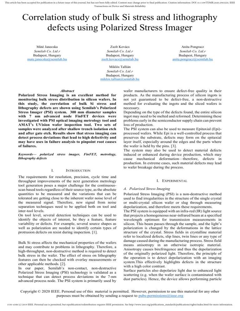
This article has been accepted for publication in a future issue of this journal, but has not been fully edited. Content may change prior to final publication. Citation information: DOI 10.1109/TDMR.2020.2965220, IEEE Transactions on Device and Materials Reliability Correlation study of bulk Si stress and lithography defects using Polarized Stress Imager Máté Janecska Semilab Co. Ltd.r Budapest, Hungary mate.janecska@semilab.hu Zsolt Kovács Semilab Co. Ltd.r Budapest, Hungary zsolt.kovacs@semilab.hu Anita Pongracz Semilab Co. Ltd.r Budapest, Hungary anita.pongracz@semilab.hu Miklós Tallián Semilab Co. Ltd.r Budapest, Hungary miklos.tallian@semilab.hu Abstract Polarized Stress Imaging is an excellent method for monitoring bulk stress distribution in silicon wafers. In this study, the correlation of bulk Si stress and lithography defects are shown using Semilab’s Polarized Stress Imager (PSI) system. 300 mm diameter samples with 7 nm advanced node FinFET devices were investigated with PSI optical imaging metrology tool and AMAT’s UVision wafer inspection tool. Two sets of samples were analyzed after shallow trench isolation etch and after gate etch. Results show that stress imaging can detect process deviations that lead to high defectivity and may have uses in failure analysis to pinpoint root causes of failures. Keywords— polarized stress imager, FinFET, metrology, lithography defects I. INTRODUCTION The requirements for resolution, precision, cycle time and throughput improvements of the next generation metrology tool generation poses a major challenge for the continuousscan based tools regardless of their source type, as the absolute quantities to be measured and the variations that can be tolerated are getting close to the inherent wafer noise level of the measured signal. Therefore, new signal from noise separation techniques need to be applied both on tool and inter-tool levels. On tool level, several detection techniques can be used to identify the objects of interest, be they a feature, feature variability or defects. For example, several source shapes as well as polarization are needed to identify certain types of protrusion defects on resist during inspection. [1]. Bulk Si stress affects the mechanical properties of the wafers and may contribute to problems in lithography. Therefore, a high-throughput, non-destructive method is required to detect bulk stress in the wafer. The effect of stress on lithography features can then be checked with overlay measurements or other applicable methods. [2]. In our paper, Semilab’s non-contact, non-destructive Polarized Stress Imaging (PSI) technology is validated as a technique that can detect process deviations in the 7-nm advanced process node. The PSI system is primarily used by wafer manufacturers to ensure defect-free quality in their products. As the manufacturing process of silicon ingots is not yet guaranteed to be defect-free, a non-destructive method for evaluating the ingots and the sliced wafers is necessary. Depending on the type of the defects found, the entire silicon ingot may need to be melted and reformed. Determining these problems early in the semiconductor supply chain can prevent loss of production. The PSI system can also be used to measure Epitaxial (Epi)processed wafers. While Epi is a well-controlled process that preserves the substrate, defects may form on the epitaxial layer itself, especially around the edges and the parts where the wafer is held by the pins. [3]. The system may also be used to detect material defects induced or enhanced during device production, which may cause mechanical deformation—therefore, defects in production. In extreme cases, such material defects may lead to wafer breakage during the process. I. EXPERIMENTAL A. Polarized Stress Imaging Polarized Stress Imaging (PSI) is a non-destructive method used to find irregularities in the structure of the single crystal or multi-crystal silicon wafer or slug through measuring depolarization, and therefore meets these requirements. The PSI system is equipped with an infra-red (IR) light source that projects a homogeneous near-infrared beam at a specified wavelength optimum for transmission measurements in silicon. This beam passes through the sample, and the light’s polarization is changed by the deformations in the lattice structure of the crystal. Stress fields in crystalline material refer to localized defects, slip lines, twin lines or any type of damage caused during the manufacturing process. Stress field means anisotropy in an otherwise isotropic material. Anisotropy causes birefringence and thus the depolarization of the originally polarized light. Therefore, the principle of the operation is to detect depolarization with an imaging system.This effectively highlights defects in the structure with a high color contrast. Surface particles also depolarize light due to enhanced light scattering (e.g. when the wafer surface is contaminated with dust particles). Hence, the device allows performing particle Copyright © 2020 IEEE. Personal use of this material is permitted. However, permission to use this material for any other purposes must be obtained by sending a request to pubs-permissions@ieee.org 1530-4388 (c) 2019 IEEE. Personal use is permitted, but republication/redistribution requires IEEE permission. See http://www.ieee.org/publications_standards/publications/rights/index.html for more information. This article has been accepted for publication in a future issue of this journal, but has not been fully edited. Content may change prior to final publication. Citation information: DOI 10.1109/TDMR.2020.2965220, IEEE Transactions on Device and Materials Reliability detection measurements on both sides simultaneously with stress measurement. The system uses a line camera with a resolution of 1×1024 pixels to create 50-μm pixel scale images of the wafer’s sections in sequence and subsequently paste them together. The resulting image consists of 36 megapixels (6000×6000 px). Fig.1: The PSI-2500, Semilab’s newly developed wafer inspection tool Tool description Wafer [mm] Loading Platform Size Semilab’s PSI PSI-2100 PSI-2500 PSI-3000 50-315 150/200/300 150/200/300 Manual Automatic/ Manual Manual Single FOUP load port capability SECS/GEM Automatic/ Manual Dual FOUP load port capability SECS/GEM and OTH Table 1. Descritpion of versions of Semilab’s PSI To create an image with a suitably high contrast, two polarizers are used perpendicularly to one another, this is called crossed polarizer position. The resulting image is referred to as the stress image. The polarizers extinguish all external lights affecting the sample, so only the defective areas are highlighted. Stress image is sufficient for finding defects on the sample. Additional parallel polarization image acquisition entails a longer measurement time but can determine the intensity of the defects, if needed. Image acquisition in parallel polarizer position: Pp Image acquisition in crossed polarizer position: Pc The amount of depolarization is calculated according to the following equation: 𝑃𝑝 − 𝑃𝑐 𝐷 = 1− 𝑃𝑝 + 𝑃𝑐 Depolarization (D) is a dimensionless quantity, and it is very close to zero. DU is used as a unit of measurement: 1 DU = 10^-6. The extent of depolarization is directly proportional to the mechanical stress in the material. Stress can be calibrated into units of Pa via optical relationships. Pa calibration is not necessary for basic application. For finding the defects, crossed polarization imaging is sufficient. Fig.2: The schematic illustration of the PSI measurement head B. UVision UVision® was developed to inspect „killer” defects down to 10 nm by AMAT. The theory of measurement based on bright-field microscopy. Bright-field technologies in wafer inspection is primary used for detecting flat pattern defects as well as three-dimensional defects. This type of defects can be voids between layers, residue materials, etc. Traditional bright-field microscopy uses multi-wavelength light sources with detectors. UVision® operates with a 266-nm-deep ultraviolet (DUV) laser light source. This light is optically shaped to line for scanning. The light reflected from the sample into separate detectors. The different channels had different purpose. One is for bright field imaging, and other for 3D inspection. After the measurement, the tool compares the intensity profile of the sites. The sites with highly different profile claimed to be sites with defects. C. Samples For the metrology qualifications and polarized stress imaging based characterization of imec’s device manufacturing processes 300 mm silicon wafers (to be converted into 7nm FinFET devices) were used. The samples represented two different stages of the process flow: STI etch wafers and Gate Etch wafers. II. RESULTS AND DISCUSSION 1) STI Etch Wafer 1530-4388 (c) 2019 IEEE. Personal use is permitted, but republication/redistribution requires IEEE permission. See http://www.ieee.org/publications_standards/publications/rights/index.html for more information. This article has been accepted for publication in a future issue of this journal, but has not been fully edited. Content may change prior to final publication. Citation information: DOI 10.1109/TDMR.2020.2965220, IEEE Transactions on Device and Materials Reliability Measurement data from STI Etch wafers is shown in figure 3 and 4. The data does not show any sign of localized or global defects on the stress measurement. Moreover, the wafers show no stress due to the gripping-releasing, stress-free sample holder. In comparison with the UVision measurements, defect inspection results from STI Etch wafers show more than 25,000 defects, with the wafer center being more defective (Fig 5.). It can be safely concluded that the etch process here did not cause a mechanical stress field in the wafer which resulted in higher amount of defects. Fig. 5: Defect map of STI Etch wafer (courtesy of Applied Materials Israel). . 2) Gate Etch Wafer Gate etch wafers were also measured in the PSI system and results are compared with UVision inspection measurements (Fig. 6-11). Fig. 3: Measured image of STI Etch wafer with crossed polarizer. Fig. 6: Measured image of Gate Etch wafer with crossed polarizer. Fig. 4: Measured image of the STI Etch wafer with parallel polarizer. Slanted stripes are side-effect of scaling the 36 Megapixel image down to fit the document format. . 1530-4388 (c) 2019 IEEE. Personal use is permitted, but republication/redistribution requires IEEE permission. See http://www.ieee.org/publications_standards/publications/rights/index.html for more information. This article has been accepted for publication in a future issue of this journal, but has not been fully edited. Content may change prior to final publication. Citation information: DOI 10.1109/TDMR.2020.2965220, IEEE Transactions on Device and Materials Reliability Further examination reveals a larger spot which is visible at around 7 o’clock position, possibly a layer delamination which causes changes in light polarization. Note that the defective area is quite large. Further investigations on the Gate Etch Wafer involved the usage of the image processing option to enhance the longrange, global stress fields. To make visibility better, contrast was also enhanced in the image below. It can be shown that possible circular, concentric intensity changes. It can’t be seen on the parallel image, therefore it must be a stress-related effect. Such a pattern was not visible in the STI Etch Wafer. Fig. 7: Measured image of Gate Etch wafer with parallel polarizer. Images of the Gate Etch Wafer reveals several interesting details. Along the edge, radial defects are clearly visible, with higher frequency between 4 o’clock and 10 o’clock positions. These defects are faintly visible to the naked eye as well, but are really highlighted on the image with crossed polarizers. These defects must originate from the Gate Etch process, as they cannot be system artefacts (the measurement is performed in x-y direction), and they are fully radial, meaning that they do not align with any Si growth direction, which would be the case for linear defects originating in the Si bulk. Fig. 8: Image of radial defects on the edge of Gate Etch Wafers Fig. 10: Stress field image of the Gate Etch Wafer showing a radial stress field. The red line shows where the line profile was measured. Defect inspection results show nearly 150,000 defects on this wafer, with their distribution closely following the distribution of the stress field (Figure 11). This may be the indication that the Gate Etch causes additional stress in the wafer, which in turn increases defectivity. Fig. 9: Defective area, possible delamination on the Gate Etch Wafer 1530-4388 (c) 2019 IEEE. Personal use is permitted, but republication/redistribution requires IEEE permission. See http://www.ieee.org/publications_standards/publications/rights/index.html for more information. This article has been accepted for publication in a future issue of this journal, but has not been fully edited. Content may change prior to final publication. Citation information: DOI 10.1109/TDMR.2020.2965220, IEEE Transactions on Device and Materials Reliability very short loop on blanket wafers without expensive patterning. ACKNOWLEDGMENT The authors are thankful for the NEMZ_15-1-2016-0020 project for supporting this work. Project no. NEMZ_15-12016-0020 has been implemented with the support provided from the National Research, Development and Innovation Fund of Hungary, financed under the NEMZ_15 funding scheme. REFERENCES [1] Yong-Kai Zhu, Gui-Yun Tian, Rong-Sheng Lu, Hong Zhang, A Review of Optical NDT Technologies, Sensors 2011, 11(8), 7773-7798 Fig. 11: Defect map of Gate Etch wafer (courtesy of Applied Materials Israel). [2] [2] Ian Stobert; Subramanian Krishnamurthy; Hongbo Shi; Scott Stiffler Model-based correction for local stress-induced overlay errors, Proceedings Volume 10587, Optical Microlithography XXXI; 105870D (2018) CONCLUSION [3] It has been shown that polarized stress imaging can detect lithography defects in the advanced process flow of 7nm FinFET devices. Running stress analysis as a screening tool could improve ramp-up of etch and deposition processes, as some of the largest defect sources could be eliminated in a [3] M. Iwabuchi, K. Mizushima, M. Mizuno, and Y. Kitagawara Dependence of Epitaxial Layer Defect Morphology on Substrate Particle Contamination of Si Epitaxial Wafer Journal of The Electrochemical Society, 147 (3) 11991203 (2000) 1530-4388 (c) 2019 IEEE. Personal use is permitted, but republication/redistribution requires IEEE permission. See http://www.ieee.org/publications_standards/publications/rights/index.html for more information.
