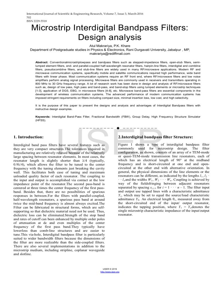
International Journal of Scientific & Engineering Research, Volume 7, Issue 3, March-2016 702 ISSN 2229-5518 Microstrip Interdigital Bandpass Filters: Design analysis Atul Makrariya, P.K. Khare Department of Postgraduate studies in Physics & Electronics, Rani Durgavati University, Jabalpur , MP, makrariya@rediffmail.com Abstract: Conventionalmicrostriplowpass and bandpass filters such as stepped-impedance filters, open-stub filters, semilumped element filters, end- and parallel-coupled half-wavelength resonator filters, hairpin-line filters, interdigital and combline filters, pseudocombline filters, and stub-line filters are widely used in many RF/microwave applications. Modern RF and microwave communication systems, specifically mobile and satellite communications required high performance, wide band filters with linear phase. Most communication systems require an RF front end, where RF/microwave filters and low noise amplifiers perform analog signal processing. Microwave filters are commonly used in receivers and transmitters operating in 800 MHz to 30 GHz frequency range. A lot of research work has been done in design and analysis of RF/microwave filters such as, design of low pass, high pass and band-pass, and band-stop filters using lumped elements or microstrip techniques [1-3], application of DGS, EBG, in microwave filters [4-8], etc. Microwave band-pass filters are essential components in the development of wireless communication systems. The advanced performance of modern communication systems has imposed stringent requirements on filters including compact size, minimal insertion loss, low cost, and high selectivity. It is the purpose of this paper to present the designs and analysis and advantages of Interdigital Bandpass filters with instructive design examples. Keywords: Interdigital Band-Pass Filter, Fractional Bandwidth (FBW), Group Delay, High Frequency Structure Simulator (HFSS). IJSER —————————— —————————— 1. Introduction: 2.Interdigital bandpass filter Structure: Interdigital band pass filters have several features such as they are very compact structures.The tolerances required in manufacturing are relatively relaxed because of the relatively large spacing between resonator elements. In most cases, the resonator length is slightly shorter than λ/4 (typically, 0.9λ/4), which allows the filter to be tuned to the center frequency with the tuning elements just breaking the cavity wall. This facilitates both case of tuning and maximum unloaded quality factor of each resonator. The coupling to the input and output is accomplished via contact at the low impedance point of the resonator.The second pass-band is centered at three times the center frequency of the first passband. Besides that, there are no possibilities of spurious responses in between.For the filters with parallel-coupled, half-wavelength resonators, a spurious pass band at around twice the mid-band frequency is almost always excited.The Filter can be fabricated in structural forms, which are selfsupporting so that dielectric material need not be used. Thus, dielectric loss can be eliminated.Strength of the stop band and rates of cutoff can been enhanced by multiple order poles of attenuation at dc and even multiples of the center frequency of the first pass band.They typically have lowerloss than comb-line structures and are easier to tune.This via-hole, Interdigital bandpass filter is particularly suited to wider bandwidth filters because the dimensions of the filter are more realizable than the side-coupled filters. There are also several implementations in addition to the microstrip medium, including stripline, coplanar waveguide and slotline. Figure 1 shows a type of interdigital bandpass filter commonly used for microstrip design. The filter configuration, as shown, consists of an array of n TEM-mode or quasi-TEM-mode transmission line resonators, each of which has an electrical length of 90° at the midband frequency and is short-circuited at one end and opencircuited at the other end with alternative orientation. In general, the physical dimensions of the line elements or the resonators can be different, as indicated by the lengths l 1 , l 2 · · · l n and the widths W1 , W2 · · · Wn . Coupling is achieved by way of the fieldsfringing between adjacent resonators separated by spacing si,i+1 for i = 1 · · · n – 1. The filter input and output use tapped lines with a characteristic admittance Y t , which may be set to equal the source/load characteristic admittance Y 0 . An electrical length θ t , measured away from the short-circuited end of the input/ output resonator, indicates the tapping position, where Y 1 = Y n denotes the single microstrip characteristic impedance of the input/output resonator. IJSER © 2016 http://www.ijser.org International Journal of Scientific & Engineering Research, Volume 7, Issue 3, March-2016 ISSN 2229-5518 703 We have studied symmetrical inter-digital band-pass filter where all microstrip resonators have equal widths i.e. Wi = W, for i = 1 to n. Using equation from 1 to 5, the characteristic admittance of the input resonator is calculated and since the inverse of the admittance is equal to the impedance,the characteristic impedance Z 1 of the input resonator is Z 1 = 1/Y 1 . For the microstrip resonator with characteristic impedance Z 1 , the width W can be calculated using following formula[6] Figure 1: Generalized schematic of an n-pole Interdigital BPF [5] This type of microstripbandpass filter is compact, but requires use of grounding microstrip resonators, which is usually accomplished with via holes. However, because the resonators are quarter-wavelength long using the grounding, the second passband of filter is centred at about three times the midband frequency of the desired first passband, and there is no possibility of any spurious response in between. 𝑊 ℎ = 1 7𝜀 +4 𝜀 +1 �2 8� 𝑟 .𝐴+ 𝑟 � 11𝜀𝑟 𝐴 while, 0.81𝜀𝑟 𝐴 = 𝑒𝑥𝑝. � (6) 𝑍1 �𝜀 + 1� − 1 42.4 𝑟 where, ε r is the dielectric constant of the substrate, h is the thickness of the substrate. 6. Electrical length θ t from the short circuited end of the input/output resonator can be obtained as [7] 𝜃𝑡 = 𝑌𝑠𝑖𝑛2 𝜃 � 𝑌0 g0 g1 𝐹𝐵𝑊 1− 2 sin−1�� (7) IJSER 7. C t i.e., the capacitance to be loaded to the input and output resonators in order to compensate for resonant frequency shift because of the effect of the tapped input and output can be calculated as [7] 3.Design steps for Interdigital band-pass filter: 1. Calculate electrical length θ for a given bandwidth FBW 𝜋 𝜃 = 2 �1 − 𝐹𝐵𝑊 2 � (1) 2. Now expressing Y in terms of Y 1 using θ as 𝑌 𝑌 = tan1 𝜃 (2) Y 1 is admittance of input line 𝑌1 𝑡𝑎𝑛𝜃 �g𝑖g𝑖+1 where, gi represents the element values of a ladder-type lowpass prototype filter with a normalized cut off frequency at Ω c =1. for i = 1 to n-1 𝑌𝑡 = 𝑌1 − 𝑌1 Now substituting Y t =1/50 and obtaining Y 1 . 1 𝑍0𝑜1,2 = 𝑌 , 1 𝑍0𝑒𝑖,𝑖+1 = 2𝑌 1 1 +𝑌1,2 1 −1⁄𝑍0𝑒 𝑖−1,𝑖−𝑌𝑖,𝑖+1 −𝑌𝑖−1,𝑖 𝑍0𝑜𝑖,𝑖+1 = 2𝑌 1 𝑖,𝑖+1 +1⁄𝑍0𝑒𝑖,𝑖+1 1 𝑍0𝑒𝑛−1,𝑛 = 𝑌 −𝑌 𝑛−1,𝑛 , for i = 2 to n-2 , for i = 2 to n-2 1 ,𝑍0𝑜𝑛−1,𝑛 = 𝑌 +𝑌 1 𝑛−1,𝑛 (9) Using above equation coupling factor can be derived as (4) 5.Calculate characteristic admittance Y t , of the tapped lines 2 𝑌1,2 8. Now the even and odd-mode impedances of the n-coupled line resonator can be determined as [8] 1 4. Calculate Y i,i+1 from J i,i+1 [5] (8) 𝑐𝑜𝑠2 𝜃𝑡 𝑠𝑖𝑛2 𝜃𝑡 � 𝑌2 0 𝑡 1 𝜔0 𝑌𝑡 � 2+ 𝑌 1 −𝑌1,2 , for i = 1 to n-1 (3) 𝑌𝑖,𝑖+1 = 𝐽𝑖,𝑖+1 sin 𝜃, cos 𝜃𝑡 𝑠𝑖𝑛3𝜃𝑡 𝑍0𝑒1,2 = 𝑌 3. Calculate J i,i+1 using following equation 𝐽𝑖,𝑖+1 = 𝐶𝑡 = (5) 𝑍0𝑒𝑖,𝑖+1 −𝑍0𝑜 𝑖,𝑖+1 𝑘𝑖,𝑖+1 = 𝑍 0𝑒𝑖,𝑖+1 +𝑍0𝑜 𝑖,𝑖+1 (10) Once the coupling factor is obtained the spacing can be obtain easily. 9. After obtaining the width and spacing of the microstrip line resonators, the equivalent length l i of the resonators can be calculated [5]. IJSER © 2016 http://www.ijser.org International Journal of Scientific & Engineering Research, Volume 7, Issue 3, March-2016 ISSN 2229-5518 𝑙𝑖 = 𝜆g0𝑖 ⁄4 − ∆𝑙𝑖 (11) Where, 𝜆g0𝑖 is the guided wavelength and ∆𝑙𝑖 is correction length of microstrip open end associated with resonator i. As the interdigital filter is symmetric therefore the guided wavelength can be obtained as 𝜆g0𝑖 = 𝜆0 (12) �𝜀𝑟𝑒 𝜀𝑟𝑒 = 𝜀𝑟+1 2 + 𝜀𝑟−1 2 �1 + 12 � 𝑊 , for W/h ≥1 (13) Now the ∆𝑙𝑖 can be determined using the empirical formula for microstrip open end validated for the range of 0.01 ≤ W/h ≤ 100 and ε r ≤ 128 given in [10] ∆𝑙𝑖 ℎ = 𝜉1 𝜉3 𝜉5 10. Now, a capacitance C t is loaded on the input and output resonators due to the tapped lines, which can be achieved by an extension in the length ∆l c of the input and output resonators which can be calculated as [5] 𝜆g01 2𝜋 tan−1 � 2𝜋𝑓0 𝐶𝑡 𝑌1 � (15) 𝑙1 = 𝑙𝑛 = 𝜆g01⁄4 − ∆𝑙1 + ∆𝑙𝐶 (16) 11. Finally the physical length l t measured from the input/output shorted end to the tapped line is calculated by [5] 𝜃 R R ∆𝜑 𝜏𝑔 = − ∆𝜔 (18) where, ∆φ is change in phase angle of |S 21 | in radians and ∆ω, is the change in frequency. It is always desirable to have a minimum and uniform group delay so as to achieve minimum signal distortion. In high speed communication system if the group delay is not uniform then the information of the signal can significantly be distorted. R R IJSER Therefore, the final lengths l 1 and l n for the input and output resonators are 𝑙𝑡 = 2𝜋𝑡 𝜆g01 To study the transmission behaviour of filter, the ׀S 21 ׀will be considered to study the fractional bandwidth (FBW). One another important filter parameter is group delay. The group delay is the measure of the time delay of the frequency spectrum of a signal. The group delay can also be defined as the rate of change of transmission phase angle with respect to frequency. Mathematically group delay can be expressed as (14) 𝜉4 ∆𝑙𝐶 = To carry out simulation for our studies, we should use driven modal solution type. The wave ports will be assigned for port excitation. An air box is created to cover the device and to provide the appropriate boundary conditions. The interdigital band-pass filter will be simulated using fast mode for a frequency range after defining an operating frequency in the HFSS model. 5.Result and Discussion: where, 𝜀𝑟𝑒 is the effective dielectric constant given by[5] −1� 2 ℎ 704 (17) Using above design steps we can obtained the design parameters for n pole interdigital band-pass filter. 4.Electromagnetic Simulation: To design and study the transmission characteristics of anpole interdigital band-pass filter, we have carried out Finite Element Method (FEM) based simulation on a proposed structure using commercial software ANSOFT HFSS v13. To create a model in HFSS as shown in Figure1, we have taken a substrate thickness in mm with dielectric constant ( ε r ) and loss tangent(tanδ) . For designing line resonators and ground we should use copper conductor with thickness in mm. The microsrip resonators were shorted to ground using via holes of radius in mm. The via-holes are filled using copper conductor of same bulk conductivity as that for the resonators and ground.The filter parameters will be calculated using the design equations and are optimized using HFSS software to achieve desired response. The final design parameters of the interdigital band-pass filter such as : Widths: W1 = W2 = W3 = W4 = W5 and Length: l 1 = l 5 and l 2 = l 3 = l 4 . Spacing: S 1,2 = S 4,5 and S 2,3 = S 3,4 and Tapping length: l t Will be calculated and all in mm. 6. Conclusion: In this paper we have studied the design step and simulation of an-pole symmetrical interdigital band-pass filter centered at a frequency of some GHz. The designs must be analyzed using existing quasi-static TEM approximations followed by simulations by finite element analysis based commercial software HFSS v13. The Group delay is a very important parameter of a filter to evaluate its performance and applicability for high speed digital systems. In most cases group delay degrades the system performance. Higher the group delay poor the performance. It will observe in the design simulation that the group delay is uniform over the entire pass band frequency. Also, we will observe that as we reduce the spacing between the line resonators, fractional bandwidth increases i.e. FBW is dependent on the coupling between the line resonators. Therefore, Interdigital BPF can find many applications in positioning, imaging, short-range high-data-rate communications systems and wireless personal area networks where the very high bandwidths are required. The Filter can be fabricated in structural forms, which are self-supporting so that dielectric material need not be used. Thus, dielectric loss can be eliminated. This viahole, Interdigital bandpass filter is particularly suited to wider bandwidth filters because the dimensions of the filter are more realizable than the side-coupled filters. 7. References: 1) J.-S. Lim, C.-S.Kim, D. Ahn, Y.-C. Jeong, and S. Nam, “Design of the low-pass filters using defected ground structure,” IEEE Transactions on Microwave Theory and Techniques, vol. 53, no. 8, pp. 2539–2545, 2005. IJSER © 2016 http://www.ijser.org International Journal of Scientific & Engineering Research, Volume 7, Issue 3, March-2016 ISSN 2229-5518 2) R.M. Kurzrok, "Design of Comb-line Bandpass Filters," IEEE Transactions on Microwave Theory and Techniques, Vol. MTT-14, July 1966, pp. 351-353. 3) J.-S. Yun, G.-Y. Kim, J.-S. Park, D. Ahn, K.-Y. Kang, and J.-B. Lim, “A design of the novel coupled line bandpass filter using defected ground structure,” IEEE MTTS International Microwave Symposium Digest, vol. 1, pp. 327–330, 2000. 4) T. Akalin, M. A. G. Laso, E. Delos, T. Lopetegi, O. Vanbesien, M. Sorolla, and D. Lippens, “High performance double-sided microstrip PBG filter,” Microwave Opt. Technol. Lett., vol. 35, no. 2, pp. 90–93, Oct. 2002. 5) Jia-Sheng Hong, “Microstrip Filters for RF/Microwave Applications”, Second Edition, published by John Wiley & Sons, Inc., New Jersey. 6) Peter A. Rizzi, “Microwave Engineering Passive Circuits”, published by Prentice Hall International, Inc., USA. 7) S. Caspi and J. Adelman, “Design of combline and interdigital filters with tapped-line input”. IEEE Transaction Microwave Theory and Techniques, 1988, 759– 763. 8) T. A. Millgan, “Dimensions of microstrip coupled lines and interdigital structures”, IEEE Transaction Microwave Theory and Techniques, 1977, 405–410. 9) Peter A. Rizzi, “Microwave Engineering Passive Circuits”, published by Prentice Hall International, Inc., USA. 10) M. Kirschning, R. H. Jansen, and N. H. L. Koster, “Accurate model for open end effect of microstrip lines”, Electronics Letters, vol. 17, 1981, 123−125. IJSER IJSER © 2016 http://www.ijser.org 705
