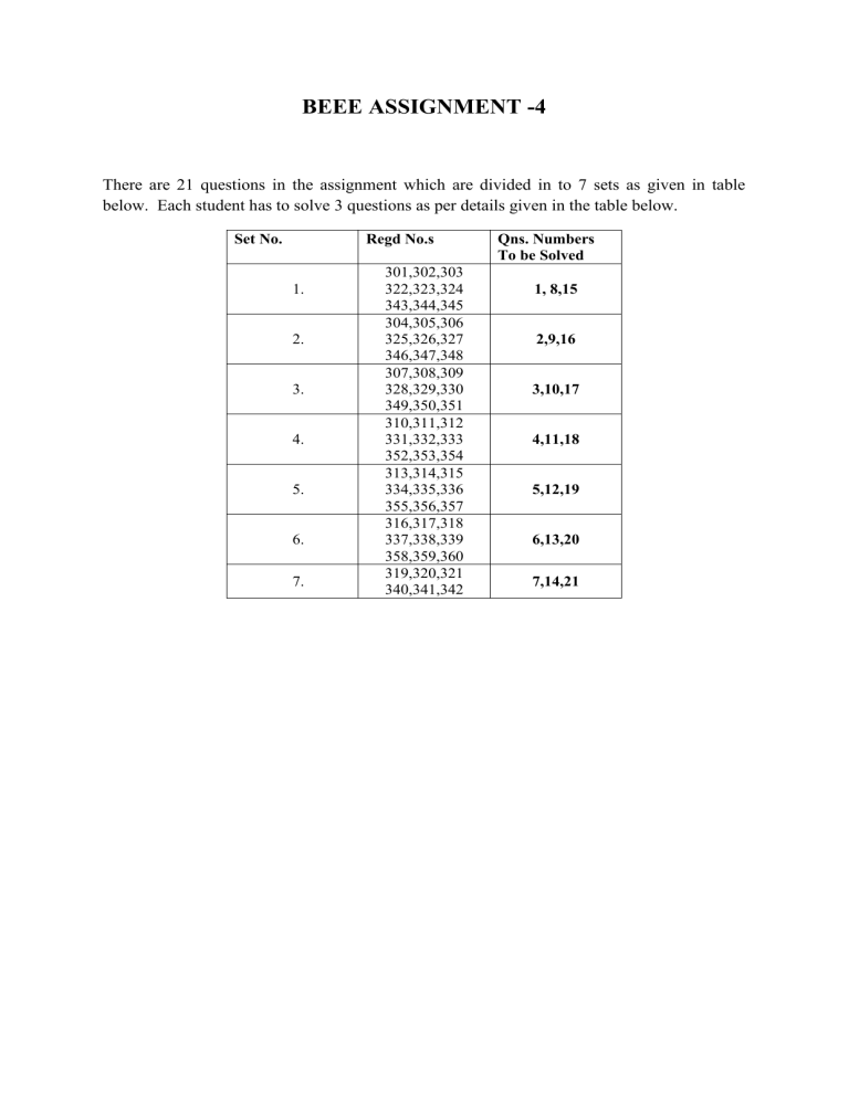
BEEE ASSIGNMENT -4 There are 21 questions in the assignment which are divided in to 7 sets as given in table below. Each student has to solve 3 questions as per details given in the table below. Set No. Regd No.s 1. 2. 3. 4. 5. 6. 7. 301,302,303 322,323,324 343,344,345 304,305,306 325,326,327 346,347,348 307,308,309 328,329,330 349,350,351 310,311,312 331,332,333 352,353,354 313,314,315 334,335,336 355,356,357 316,317,318 337,338,339 358,359,360 319,320,321 340,341,342 Qns. Numbers To be Solved 1, 8,15 2,9,16 3,10,17 4,11,18 5,12,19 6,13,20 7,14,21 1. a) What is semiconductor? How does energy band structure of a semiconductor differ from those of a conductor and an insulator? b) Define doping. Explain how n-type and p-type semiconductors are formed. [6M+6M] 2. a) Describe a majority and minority charge carriers. b) What is PN junction? Discuss its formation.[6M+6M] 3. a) List out the applications of PN junction diode. b) Write short notes on extrinsic semi-conductor. [6M+6M] 4. Draw the V-I characteristic of Zener diode and explain its operation.[12M] 5. a) Discuss the operation of half-wave rectifier with neat diagram. b) Discuss the operation of full-wave centre tapped rectifier with neat diagram. [6M+6M] 6. Discuss the operation of bridge rectifier with neat diagrams.[12M] 7. 8. a) Explain the operation of PNP transistor. b) Explain how transistor is used as an amplifier. 9. [6M + 6M] 10. 11. a) Explain how materials are classified based on energy band theory. b) List out any 3 differences between two types of full wave rectifier. [6M + 6M] 12. Derive the following for Half Wave rectifier: i)Average value of output voltage ii)R.M.S output voltage iii) Ripple factor and iv) P.I.V[3M+3M+3M+3M] 13. Derive the following for Full Wave centre tapped rectifier: i) Average value of output voltage ii) R.M.S output voltage iii) Ripple factor and iv) P.I.V[3M+3M+3M+3M] 14. Derive the following for Full Wave Bridge rectifier: i)Average value of output voltage ii)R.M.S output voltage iii) Ripple factor and iv) P.I.V[3M+3M+3M+3M] 15. a) Explain different types of Transistors in detail. b) Derive the relation for `Base current: Emitter current: Collector current` in terms of `alpha` in a transistor. [6M + 6M] 16. Draw the circuit for the CE configuration of a transistor and explain in brief its input and output characteristics.[12M] 17. Draw and explain the characteristics of transistor in CB configuration.[12M] 18. A voltage of 200 Sin(ωt) is applied to a) Half wave rectifier b) Full wave rectifier With load resistance of 5 k ohms. Find the maximum DC current component, RMS Voltage and ripple factor in both the cases.[6M + 6M] 19. A voltage of 100 Sin(ωt) is applied to a) Half wave rectifier b) Full wave rectifier With load resistance of 1 k ohms. Find the maximum DC current component, RMS Voltage and ripple factor in both the cases. [6M + 6M] 20. 21.
