Light Emission and Charge Trapping in Er Doped Silicon
advertisement

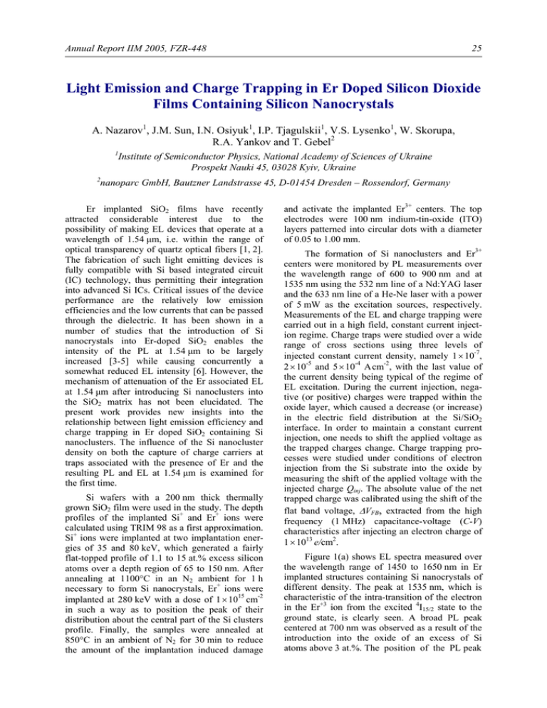
Annual Report IIM 2005, FZR-448 25 Light Emission and Charge Trapping in Er Doped Silicon Dioxide Films Containing Silicon Nanocrystals A. Nazarov1, J.M. Sun, I.N. Osiyuk1, I.P. Tjagulskii1, V.S. Lysenko1, W. Skorupa, R.A. Yankov and T. Gebel2 1 2 Institute of Semiconductor Physics, National Academy of Sciences of Ukraine Prospekt Nauki 45, 03028 Kyiv, Ukraine nanoparc GmbH, Bautzner Landstrasse 45, D-01454 Dresden – Rossendorf, Germany Er implanted SiO2 films have recently attracted considerable interest due to the possibility of making EL devices that operate at a wavelength of 1.54 µm, i.e. within the range of optical transparency of quartz optical fibers [1, 2]. The fabrication of such light emitting devices is fully compatible with Si based integrated circuit (IC) technology, thus permitting their integration into advanced Si ICs. Critical issues of the device performance are the relatively low emission efficiencies and the low currents that can be passed through the dielectric. It has been shown in a number of studies that the introduction of Si nanocrystals into Er-doped SiO2 enables the intensity of the PL at 1.54 µm to be largely increased [3-5] while causing concurrently a somewhat reduced EL intensity [6]. However, the mechanism of attenuation of the Er associated EL at 1.54 µm after introducing Si nanoclusters into the SiO2 matrix has not been elucidated. The present work provides new insights into the relationship between light emission efficiency and charge trapping in Er doped SiO2 containing Si nanoclusters. The influence of the Si nanocluster density on both the capture of charge carriers at traps associated with the presence of Er and the resulting PL and EL at 1.54 µm is examined for the first time. Si wafers with a 200 nm thick thermally grown SiO2 film were used in the study. The depth profiles of the implanted Si+ and Er+ ions were calculated using TRIM 98 as a first approximation. Si+ ions were implanted at two implantation energies of 35 and 80 keV, which generated a fairly flat-topped profile of 1.1 to 15 at.% excess silicon atoms over a depth region of 65 to 150 nm. After annealing at 1100°C in an N2 ambient for 1 h necessary to form Si nanocrystals, Er+ ions were implanted at 280 keV with a dose of 1 × 1015 cm-2 in such a way as to position the peak of their distribution about the central part of the Si clusters profile. Finally, the samples were annealed at 850°C in an ambient of N2 for 30 min to reduce the amount of the implantation induced damage and activate the implanted Er3+ centers. The top electrodes were 100 nm indium-tin-oxide (ITO) layers patterned into circular dots with a diameter of 0.05 to 1.00 mm. The formation of Si nanoclusters and Er3+ centers were monitored by PL measurements over the wavelength range of 600 to 900 nm and at 1535 nm using the 532 nm line of a Nd:YAG laser and the 633 nm line of a He-Ne laser with a power of 5 mW as the excitation sources, respectively. Measurements of the EL and charge trapping were carried out in a high field, constant current injection regime. Charge traps were studied over a wide range of cross sections using three levels of injected constant current density, namely 1 × 10⁻⁷, 2 × 10⁻⁵ and 5 × 10⁻⁴ A cm-2, with the last value of the current density being typical of the regime of EL excitation. During the current injection, negative (or positive) charges were trapped within the oxide layer, which caused a decrease (or increase) in the electric field distribution at the Si/SiO2 interface. In order to maintain a constant current injection, one needs to shift the applied voltage as the trapped charges change. Charge trapping processes were studied under conditions of electron injection from the Si substrate into the oxide by measuring the shift of the applied voltage with the injected charge Qinj. The absolute value of the net trapped charge was calibrated using the shift of the flat band voltage, ∆VFB, extracted from the high frequency (1 MHz) capacitance-voltage (C-V) characteristics after injecting an electron charge of 1 × 10¹³ e/cm2. Figure 1(a) shows EL spectra measured over the wavelength range of 1450 to 1650 nm in Er implanted structures containing Si nanocrystals of different density. The peak at 1535 nm, which is characteristic of the intra-transition of the electron in the Er+3 ion from the excited 4I15/2 state to the ground state, is clearly seen. A broad PL peak centered at 700 nm was observed as a result of the introduction into the oxide of an excess of Si atoms above 3 at.%. The position of the PL peak 26 A. Nazarov et al.; Light Emission and Charge Trapping … Fig. 1: (a) Electroluminescence (EL) spectra of the ITOSiO2-Si structures with SiO2 containing Si nanoclusters and Er; (b) PL and EL intensity at 1535 nm wavelength and PL intensity at 707 nm wavelength in dependence on excess Si content. did not change with increasing Si concentration and corresponds to the formation of Si nanoclusters with a mean size of about 3 nm [7]. The relative PL intensity of the emission peak of the Si nanocrystals and the peak at 1535 nm due to the presence of Er3+ ions are shown in Fig. 1(b). One can see that the increase in Si nanocluster density results in an increased PL intensity of the infrared peak from Er3+. A maximum value is observed at the excess Si content of 10 at.% . In contrast, the EL intensity at 1535 nm is strongly quenched at such an excess silicon concentration. It should be noted that the intensity of the infrared EL diminishes strongly with decreasing the average distance between the silicon clusters below the mean free path of the hot electrons (or heat up distance), which equals to approximately 3 nm [8]. Our calculations show that for Si nanoclusters with a mean size of 3 nm, the average distance between the nanoclusters becomes smaller than 3 nm for an excess Si content of more than 5 at.% (see Fig. 1(b)). Thus the average energy of the electrons will decrease with increasing the fraction of direct tunneling among the silicon nanoclusters. It should also be noted that in our case EL from Si nanoclusters has not been observed at the currents and voltages used, up to the breakdown of the dielectric. This can serve as evidence of the ineffective excitation of the Si nanoclusters by the high energy injected electrons. Due to the inefficient excitation of silicon nanoclusters, the EL from the Er centers can not be efficiently excited through the strong energy transfer from the excited silicon clusters to the Er centers compared with the PL excitation processes. The current density, J, versus inverse electric field, E, was plotted in Fowler-Nordheim (FN) coordinates (ln(J/E2)-1/E) for different values of the excess Si content as shown in Fig. 2. The cha- Fig. 2: Injected current density divided by the square of the electric field versus the reciprocal electric field in the ITOSi-rich SiO2:Er-Si MOS structure with different excess Si concentrations. racteristics so obtained reveal that up to a 3 at.% excess Si content the current injection through the dielectric can be described by the Fowler-Nordheim electron tunneling mechanism [9]. For a higher concentration of the excess Si atoms of 5.6 at.%, the effective potential barrier for FN tunneling decreases from 3.15 to 2.90 eV. This points to the influence of trapping on the electron tunneling through the triangular potential barrier from Si to the SiO2 conduction band, the so-called trap-assisted tunneling mechanism [10]. At a higher excess Si content the transition from FN tunneling to direct tunneling between silicon clusters can be clearly seen (Fig. 2). The dependence of the trapped charge on the injected electron charge is shown in Fig. 3. The starting unimplanted oxide exhibits practically no charge trapping following electron injection at a charge density of 1013 e / cm2. After the same amount of injection the Er+ implanted sample shows considerable positive charge trapping. This indicates the presence of hole traps with a giant cross-section (σh0 > 10-13 cm2) in the Er-implanted oxide. The subsequent introduction into the Erimplanted oxide of Si nanoclusters results in additional electron trapping and points towards the formation of negative charge traps with a giant cross-section (σe0 > 10-13 cm2). Furthermore, an increase in the Si nanoclusters density up to 15 % is accompanied by an increased magnitude of the trapped negative charges (see inset to Fig. 3). Computer data processing of the COX∆VCC vs. Qinj curves was done on the basis of the model for the first order charge carrier trapping [11, 12]: Qit = Qit max [1 – exp(-σi Qinj)] , where Qit and Qit max are respectively the trapped and the maximal trapped charge at the ith trap, andσi is the cross-section of the ith trap. The most Annual Report IIM 2005, FZR-448 Fig. 3: Net trapped charge calculated from the change in voltage applied to the ITO-SiO2-Si structure in a constant current regime as a function of injection charge from the Si substrate, for Er and Si implanted SiO2. Inset: Charge on the traps with capture cross-section of more than 10-13 cm2 as a function of excess Si content. important findings may be summarized as follows. The starting structure exhibits only hole traps with cross-sections σh1 ≈ 6.2 × 10⁻¹⁵ cm2, σh2 ≈ 1.2 × 10⁻¹⁵ cm2 and σh3 ≈ 4.7 × 10⁻¹⁷ cm2. The implantation of Er, apart from hole traps of a giant cross-section (> 10-13 cm2), introduces into the oxide an appreciable concentration of electron traps of a large cross-section σe1 ≈ 7.0 × 10⁻¹⁴ cm2 and σe2 ≈ 7.0 × 10⁻¹⁵ cm2 as well as a specific pair of electron and hole traps with similar cross-sections σeEr ≈ 3.0 × 10⁻¹⁸ cm2 and σhEr ≈ 6.0 × 10⁻¹⁸ cm2, respectively. The additional implantation of Si, resulting in the formation of Si nanoclusters, apart from creating electron traps of a giant cross-section, increases too the concentration of electron traps with the following cross-sections: σe2 ≈ 7 × 10-15 сm2 and σe1 ≈ 7 × 10-14 сm2, -15 2 σe3 ≈ 1.5 × 10 сm . However, as the concentration of the extra Si exceeds 5.6 at.%, the capture of electrons at these traps shows a dramatic decrease (see Fig. 3). For excess Si concentrations above 3 at.%, there is also a considerable reduction in the charge trapping at the electron/hole trap pair of a small cross-section (∼ 10-18 cm2) that is formed following the implantation of Er. Thus, it is believed that large Er inclusions, which trap effectively positive charge, create in their vicinity defects that can capture electrons. The introduction of Si nanocrystals into the matrix enhances the process of electron trapping at these crystallites as well as in the presumably disordered surroundings, which may lead to Coulomb scattering of the injected electrons and attenuation of their interaction with the Er centers around them. Since the excitation of the Er through the excitation of the Si clusters is not efficient in the EL process, we suggest that Er excitation is mainly due to direct impact excitation of hot electrons [13], 27 Fig. 4: EL intensity vs. current density for an ITO-Si-rich SiO2:Er-Si MOS structure for different concentrations of the excess Si atoms. Inset: The στ as a function of excess Si content calculated from the data presented in Fig. 4 using the expression EL=ELmax στJ/( στJ+1), where the τ is the overall lifetime of the Er, and σ is the excitation crosssection of the Er centers. which are accelerated by the high electric field in the SiO2 conduction band after FN tunnelling injection from the Si substrate. The scattering of hot electrons by both the charged defects and the Si nanoclusters results in a reduction of the average energy and the average impact excitation cross section of the Er centres around the negatively charged nanoclusters. Increasing the Si nanocrystal density (for concentrations of the excess Si larger than 5 at.%) alters the conductance from FN tunnelling to direct tunnelling through silicon clusters. The tunnelling electrons have insufficient energy to excite Er centres, which subsequently reduces the EL efficiency. The defect influence on the product of the effective electron life time (τ) and the effective cross-section of excitation (σ) can be estimated from the dependence of the EL intensity on current density [6] in Fig. 4. As can be seen from the inset to Fig. 4, the value στ decreases about seven times with increasing excess Si content from 1.1 to 15 at.%. In a study [3] of the dependence of the Er luminescence decay time on the excess Si concentration from 2.4 to 11 at.% after annealing at the same temperature of 1100°C, the lifetime of the Er-induced PL was found to decrease only by a factor of about 2 (from 4.4 to 2.1 ms). This means that the excitation cross section of Er was reduced by a factor of more than 3 in the EL excitation by introducing Si clusters with an excess Si content of up to 15 at.%. Such different behavior of the PL and EL depending on the Si nanocrystals density is associated primarily with the different nature of the excitation in the vicinity of the Er3+ ion. In the PL excitation process, the excitation of Er occurs via naturally charged exciton relaxation created in the Si nanoclusters, which does not alter significantly 28 A. Nazarov et al.; Light Emission and Charge Trapping … the electric field around the Si nanocrystals. In the EL excitation process, electrons trapped at the Si nanoclusters act repulsively to the hot electrons for excitation of both of the nanoclusters and the Er centers in the surroundings. This could be one of the reasons for the insufficient excitation of both the EL from nanoclusters and the Er centers with introducing discrete Si clusters. The larger the number of the Si nanocrystals surrounding an Er inclusion, the more efficient screening of the electric field among the clusters occurs, which is essential for the heating of electrons. Consequently, in considering the excitation of Er ions by electrons passing through an amorphous SiO2 layer, one should take into account their interaction with the defect environment of the Er inclusions. In conclusion, it has been found that the introduction of Si nanocrystals results in the creation of negative charge traps of a giant cross-section, which can scatter efficiently “hot” electrons. Higher concentrations of the Si nanoclusters alter the mechanism of current passage through the dielectric. In this case, electrons are most likely transported in the SiO2 via Si nanocluster mediated tunnelling, and therefore they interact very little with the Er inclusions. The presented results have been recently published as A. Nazarov et al., Appl. Phys. Lett. 86 (2005) 151914. References [1] L. Pavesi, J. Phys.: Condens. Matter 15 (2003) R1169 [2] M. Sopinskyy, V. Khomchenko, Current Opinion in Solid State and Materials Sci. 7 (2003) 97 [3] M. Fujii, K. Imakita, K. Watanabe, S. Hayashi, J. Appl. Phys. 95 (2004) 272 [4] K. Watanabe, M. Fujii, S. Hagashi, J. Appl. Phys. 90 (2001) 4761 [5] A.J. Kenyon, C.E. Chryssou, C.W. Pitt, T. Shimizu-Iwayama, D.E. Hole, N. Sharma, C.J. Humphreys, J. Appl. Phys. 91 (2002) 367 [6] M.E. Castagna, S. Coffa, M. Monaco, L. Caristia, A. Messina, R. Mangano, C. Bongiono, Physica E 16 (2003) 547 [7] B. Garrido, M. Lopez, C. Garcia, A. Perez-Rodriduez, J.R. Morante, C. Bonafos, M. Carrada, A. Claverie, J. Appl. Phys. 91 (2002) 798 [8] D.J. DiMaria, T.N. Theis, J.R. Kirtley, F.L. Pesavento, D.W. Dong; S.D. Brorson, J. Appl. Phys. 57 (1985) 1214 [9] Z.A. Weinberg, J. Appl. Phys. 53 (1982) 5052 [10] S. Fleischer, P.T. Lai, Y.C. Cheng, J. Appl. Phys. 72 (1992) 5711 [11] V.V. Afanas’ev, V.K. Adamchuk, Prog. Surf. Sci. 47 (1994) 301 [12] A.N. Nazarov, T. Gebel, L. Rebohle, W. Skorupa, I.N. Osiyuk, V.S. Lysenko, J. Appl. Phys. 94 (2003) 4440 [13] Y.S. Han, S.Y. Seo, J.H. Shin, Appl. Phys. Lett. 79 (2001) 178

![Solution to Test #4 ECE 315 F02 [ ] [ ]](http://s2.studylib.net/store/data/011925609_1-1dc8aec0de0e59a19c055b4c6e74580e-300x300.png)

