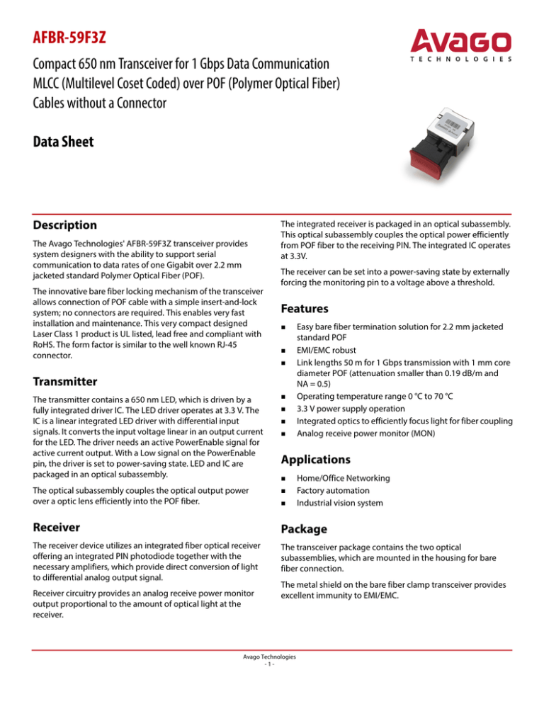
AFBR-59F3Z
Compact 650 nm Transceiver for 1 Gbps Data Communication
MLCC (Multilevel Coset Coded) over POF (Polymer Optical Fiber)
Cables without a Connector
Data Sheet
Description
The Avago Technologies' AFBR-59F3Z transceiver provides
system designers with the ability to support serial
communication to data rates of one Gigabit over 2.2 mm
jacketed standard Polymer Optical Fiber (POF).
The innovative bare fiber locking mechanism of the transceiver
allows connection of POF cable with a simple insert-and-lock
system; no connectors are required. This enables very fast
installation and maintenance. This very compact designed
Laser Class 1 product is UL listed, lead free and compliant with
RoHS. The form factor is similar to the well known RJ-45
connector.
The integrated receiver is packaged in an optical subassembly.
This optical subassembly couples the optical power efficiently
from POF fiber to the receiving PIN. The integrated IC operates
at 3.3V.
The receiver can be set into a power-saving state by externally
forcing the monitoring pin to a voltage above a threshold.
Features
Transmitter
Easy bare fiber termination solution for 2.2 mm jacketed
standard POF
EMI/EMC robust
Link lengths 50 m for 1 Gbps transmission with 1 mm core
diameter POF (attenuation smaller than 0.19 dB/m and
NA = 0.5)
Operating temperature range 0 °C to 70 °C
3.3 V power supply operation
Integrated optics to efficiently focus light for fiber coupling
Analog receive power monitor (MON)
The transmitter contains a 650 nm LED, which is driven by a
fully integrated driver IC. The LED driver operates at 3.3 V. The
IC is a linear integrated LED driver with differential input
signals. It converts the input voltage linear in an output current
for the LED. The driver needs an active PowerEnable signal for
active current output. With a Low signal on the PowerEnable
pin, the driver is set to power-saving state. LED and IC are
packaged in an optical subassembly.
The optical subassembly couples the optical output power
over a optic lens efficiently into the POF fiber.
Receiver
Package
The receiver device utilizes an integrated fiber optical receiver
offering an integrated PIN photodiode together with the
necessary amplifiers, which provide direct conversion of light
to differential analog output signal.
The transceiver package contains the two optical
subassemblies, which are mounted in the housing for bare
fiber connection.
Receiver circuitry provides an analog receive power monitor
output proportional to the amount of optical light at the
receiver.
Applications
Home/Office Networking
Factory automation
Industrial vision system
The metal shield on the bare fiber clamp transceiver provides
excellent immunity to EMI/EMC.
Avago Technologies
-1-
AFBR-59F3Z
Data Sheet
Pin Description and Recommended PCB Footprint
Pin Description and Recommended PCB
Footprint
The EMI shield and the additional ground pins (11,12,13, and
14) are isolated from the internal circuit of the transceiver and
are to be connected to equipment chassis ground.
AFBR-597F3Z has ten active signal pins (including supply
voltage and ground pins), two EMI shield solder posts, two
additional ground pins and two mounting posts, which exit at
the bottom of the housing.
Table 1 Pin Descriptions
Pin No.
Name
Symbol Pin No.
Name
Symbol
1
Data Input (Negative)
TDN
8
Imon/Rx_En
IMON/Rx_EN
2
Data Input (Positive)
TDP
9
Data Output (Negative)
RDN
3
Ground Tx
GND
10
Data Output (Positive)
RDP
4
Supply Voltage Tx
Vdd
11
Chassis GND
5
Tx_ Enable
Tx_En
12
Chassis GND
6
Supply Voltage Rx
Vdd
13
Chassis GND
7
Ground Rx
GND
14
Chassis GND
0
0.76
2.03
3.3
4.57
5.84
Figure 1 PCB Footprint and Pin-out Diagram
Top View
Dia
me
ter
0.8
(10
×)
7.74
2
4
3
5
7
m
5.2
4.0
1
8
6
Dia
10
12
11
ter 3.2
Diame
Diam
eter
0
2.74
r1
ete
)
2×
.3 (
9
1.3
13
(2×)
Mount Post
Unplated (2×)
(2×
)
14
Outer edge housing
ź
7.83 5.83 3.89
FRONT
Dimension: mm
Recommended PCB thickness: 1.57 ± 0.08
ź
0
Recommended Compliance Table
Feature
Test Method
Performance
Electrostatic discharge (ESD) to the electrical pins
JESD22-A114
Withstands up to 2 kV HBM applied between the electrical pins.
Eye safety
EN 60825-1:52007
Laser Class 1 product (LED radiation only).
Avago Technologies
-2-
AFBR-59F3Z
Data Sheet
Absolute Maximum Ratings
Absolute Maximum Ratings
Stresses in excess of the absolute maximum ratings can cause catastrophic damage to the device. Limits apply to each parameter in
isolation, all other parameters having values within the recommended operation conditions. It should not be assumed that limiting
values of more than one parameter can be applied to the products at the same time. Exposure to the absolute maximum ratings for
extended periods can adversely affect device reliability.
Parameter
Symbol
Min.
Max.
Units
Supply Voltage
Vdd Max
–0.5
4.5
V
Storage Temperature
TSTG
–40
85
°C
Lead Soldering Temperature a
Tsold
260
°C
Lead Soldering Timea
tsold
10
s
Electrostatic Voltage Capabilityb
ESD
2.0
kV
Installation Temperaturec
TI
50
°C
0
a.
The transceiver is Pb-free wave solderable. According to JEDEC J-STD-020D, the moisture sensitivity classification is
MSL2a.
b.
ESD Capability for all Pins HBM (human body model) according JESD22-A114B.
c.
Temperature range over which fibers can be connected or disconnected to or from the bare fiber clamp.
Recommended Operating Conditions
Parameter
Symbol
Min.
Typ.
Max.
Units
Operating Temperature
TA
0
25
70
°C
DC Supply Voltage
VDD
3.14
3.30
3.47
V
NOTE
All the data in this specification refers to the operating conditions above and over lifetime, unless otherwise stated.
Mechanical Characteristics
Parameter
Min.
Typ.
Max.
30
Fiber/Cable Retention Forcea
15
Clamp Opening Force
N
50
20
10
Clamp Closing Force
30
13
5
Units
20
Temp. (°C)
25
N
0...70
N
25
N
0....50b
N
25
N
0....50b
a.
Measured with Avago’s AFBR-HUDxxxZ (2.2 mm duplex-fiber, PE-jacket, without connector) with 100 mm/ min traction speed.
b.
Temperature range over which fibers can be connected or disconnected to or from the bare fiber clamp.
Avago Technologies
-3-
AFBR-59F3Z
Data Sheet
Transmitter Electrical Characteristics
Transmitter Electrical Characteristics
Parameter
Symbol
Current Consumption
Idd
Current Consumption – disabled
Idd, Dis
Symbol Rate
SR
Input Impedance to GND
ZIN, SE
Common Mode input voltage
VIN, CM
Differential Input Voltage Swinga
VIN,DIFF
Transmitter Enable Input Low Voltageb
VIL
Transmitter Enable Input High Voltageb
VIH
Min.
0.4
Typ.
Max.
47
55
mA
0.6
0.8
mA
312.5
MSps
64
190
Units
240
300
mV
960
1200
mVpk-pk
–0.3
0.8
V
2.0
VDD+0.3
V
a.
To avoid clipping, the differential input amplitude swing must not exceed 4 × VCM.
b.
The transmitter enable PIN has an internal pull-up resistor.
Transmitter Optical Characteristics
Parameter
Symbol
Min.
Central Wavelength
lC
Spectral Bandwidth (RMS)
Dl
Average Output Power [3]
P
–6.0
ER
8
Extinction Ratio [3]
635
Typ.
650
–2.1
Max.
Units
675
nm
17
nm
0.5
dBm
10
dB
a, b
Optical Rise Time (10%–90%)
tR
2.3
4.0
ns
Optical Fall Time (90% –10%) a, b
tF
2.6
4.0
ns
a.
Measured with binary modulation at a data rate of 125 MBd and with typical VIN,CM and VIN,DIFF. The output power coupled into the POF is
measured with a large area detector at the end of 1 m POF with NA = 0.5, which is ideally coupled to the transmitter.
b.
Measured with 62.5 MHz square signal.
Avago Technologies
-4-
AFBR-59F3Z
Data Sheet
Receiver Electrical Characteristics
Receiver Electrical Characteristics
Parameter
Symbol
Min.
Typ.
Max.
Units
Current Consumption
Idd
12
14
20
mA
Current Consumption – Disabled
Idd, Dis
0.5
0.7
0.9
mA
Output Common Mode Voltage
VOUT, CM
1.18
1.23
1.28
V
Differential Output Voltage Swing a
VOUT,DIFF
180
240
300
mVpk-pk
Single-Ended Output Resistance
ZOUT,SE
75
Differential Output Resistance
ZOUT,DIFF
150
Startup Time from Powersaving
tON
300
ns
Shutdown Time to Powersaving
tOFF
125
ns
Monitoring Output/Optical Input
IMON/ Pin
0.23
A/W
Max. Monitor Voltageb
VMON,MAX
Input Voltage for Power Save Mode
VMON,PS-TH
1.3
V
1.8
V
a.
Conditions: Extinction ratio of optical input signal equal to 10 dB, differential load=150 .
b.
Monitor current is limited by VMON,MAX/Load resistance.
Receiver Optical Characteristics
Parameter
Central Wavelength
Symbol
C
Min.
635
Typ.
650
Max.
675
Units
nm
Informative Section
Avago cannot guarantee the following parameters and values because they also depend on the performance of the PHY chips.
However, you can use them to calculate the 1 Gbps link budget. Furthermore, you can use them to gauge link performance.
Transmitter Optical Characteristics
Parameter
Average Output Power for 1 Gbpsa
a.
Symbol
POUT 1Gbps
Min.
–5.8
Typ.
–1.9
Max.
0.7
Units
dBm
1 Gbps transmission based on PAM16 modulation. Tested with KDPOF KD1001 PHY-IC.
Unstressed Receiver Optical Characteristics
Parameter
Receiver Input Power for 1 Gbpsa, b
Symbol
Pin 1Gbps Min
Min.
–17.5
a.
1 Gbps transmission based on PAM16 modulation. Tested with KDPOF KD1001 PHY-IC.
b.
Only optical attenuator is used to degrade the optical input test signal to the receiver.
Avago Technologies
-5-
Typ.
Max.
3
Units
dBm
AFBR-59F3Z
Data Sheet
Link Performance
Link Performance
Parameter
Link distancea, b
Symbol
l
Min.
50
Typ.
Max.
Units
m
a.
1 Gbps transmission based on PAM16 modulation. Tested with KDPOF KD1001 PHY-IC.
b.
POF parameters: attenuation smaller than 0.19 dB/m, 1 mm core diameter and NA of 0.5. Direct connection between Tx and Rx without
inline connector or any additional attenuation.
Avago Technologies
-6-
AFBR-59F3Z
Data Sheet
Mechanical Data – Package Outline
Mechanical Data – Package Outline
2.54 (6×)
2.54
4.0 ± 0.15
5.2
9.4 ± 0.2
0
2.74
6.65
1.52
7.78
11.65
1.27 (8×)
Figure 2 Package Outline Drawing
15.9 ± 0.15
4.9
6
3
11.4
10.85 ± 0.2
0.9 ± 0.15
3.75 ± 0.2
0.25 ± 0.05 (10×)
0.25 ± 0.05
2.6
0.5 ± 0.05 (10×)
15.8 ± 0.2
15
Notes:
1. Dimension: mm
2. General tolerance: ±0.1
3. Recommended PCB thickness: 1.57 ± 0.08
4. Design related is a small gap between plastic part and
dust plug possible. Function is nevertheless given.
24.4 ± 0.25
Clamp open
Clamp with Dust Plug
+0.4 [4]
12 ± 0.2
15.5 ± 0.25
29.2 -0.2
Avago Technologies
-7-
AFBR-59F3Z
Data Sheet
Application Circuit
Application Circuit
The recommended application circuit is shown in Figure 3. It shows the minimum external circuitry at DC-coupling for the
connection of the AFBR-59F3Z to the KDPOF 1001-PHY.
Figure 3 Application Circuit with KDPOF KD1001 PHY-IC Configuration
AFBR-59F3Z
[1]
OFE_RXP
237:
RDP
[1]
OFE_RXN
RDN
Imon/Rx_EN
OFE_PMON
OFE_Rx_EN_N
GND
[3]
10 μF
10 μF
100 nF
GND
Vdd
Rx
Tx_EN
Tx
3.3V
KDPOF1001-PHY
1 μH
GND
Tx_EN OUT
3.3V
1 μH
10 μF
100 nF
10 μF
GND
GND
TxOUT_P
TDP
[2]
TxOUT_N
Vdd
TDN
[2]
Chassis GND
NOTE
1.
Single-ended output impedance, ZOUT,SE = 75 .
2.
Single-ended input impedance, ZIN,SE = 64 .
3.
Choose a suitable resistor value such that the output monitor voltage is not saturated. See Figure 4.
Figure 4 depicts the relationship between monitor voltage and POF length with 10 k, 20 k, and 47 k.
Figure 4 Typical Vmon vs. POF Length
Monitor voltage vs. POF length
1.6
1.4
1.2
Vmon (V)
1
0.8
Vmon(10k)
0.6
Vmon(20k)
Vmon(47k)
0.4
0.2
0
60
50
40
30
POF length (m)
20
10
0
Avago Technologies
-8-
For product information and a complete list of distributors, please go to our web site:
www.avagotech.com
Avago Technologies and the A logo are trademarks of Avago Technologies in the United
States and other countries. All other brand and product names may be trademarks of their
respective companies.
Data subject to change. Copyright © 2014–2016 Avago Technologies. All Rights Reserved.
AV02-4655EN – March 16, 2016
