Diode Circuit Analysis Exam - İzmir Economics University
advertisement
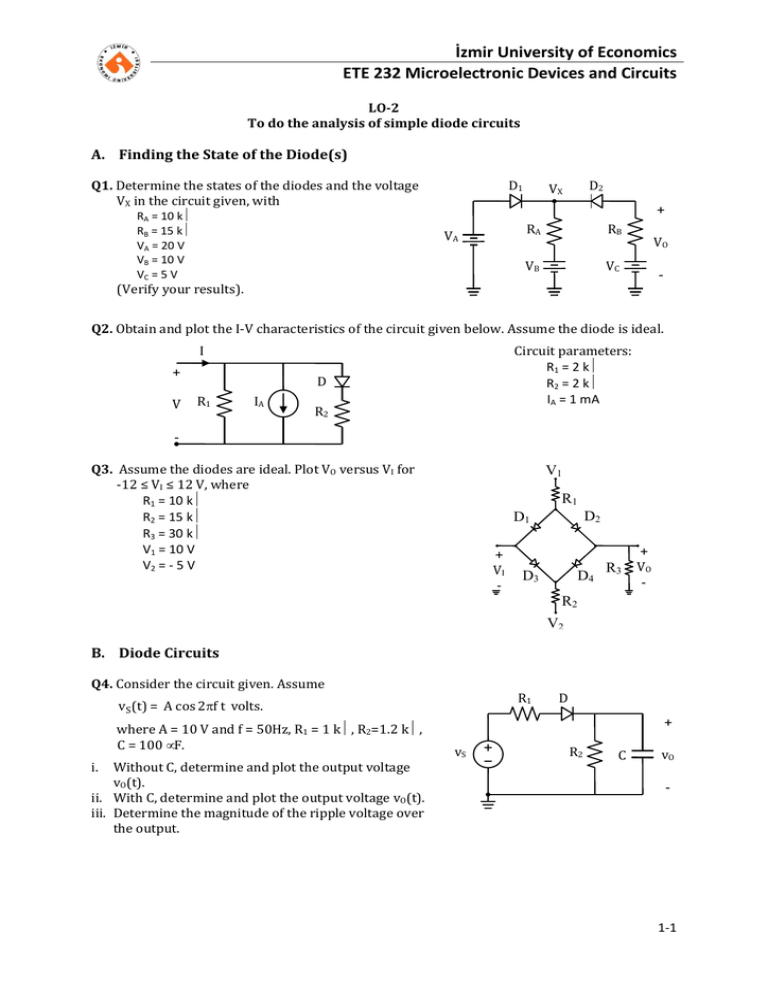
İzmir University of Economics ETE 232 Microelectronic Devices and Circuits LO-2 To do the analysis of simple diode circuits A. Finding the State of the Diode(s) D1 Q1. Determine the states of the diodes and the voltage VX in the circuit given, with RA = 10 kΩ RB = 15 kΩ VA = 20 V VB = 10 V VC = 5 V D2 VX + RA VA RB VO VB VC - (Verify your results). Q2. Obtain and plot the I-V characteristics of the circuit given below. Assume the diode is ideal. I + V Circuit parameters: R1 = 2 kΩ R2 = 2 kΩ IA = 1 mA D R1 IA R2 Q3. Assume the diodes are ideal. Plot VO versus VI for -12 ≤ VI ≤ 12 V, where R1 = 10 kΩ R2 = 15 kΩ R3 = 30 kΩ V1 = 10 V V2 = - 5 V V1 R1 D2 D1 + + VI - D3 D4 R3 VO - R2 V2 B. Diode Circuits Q4. Consider the circuit given. Assume R1 vS (t) = Acos 2πf t volts. where A = 10 V and f = 50Hz, R1 = 1 kΩ, R2=1.2 kΩ, C = 100 µF. Without C, determine and plot the output voltage vO(t). ii. With C, determine and plot the output voltage vO(t). iii. Determine the magnitude of the ripple voltage over the output. D + vS R2 C vO i. - 1-1 Q5. Design a circuit to generate a steady state voltage vO(t) from the input voltage vS(t) as given below. Circuit to be designed VS + 1V vS,volts t VO -1 V 2 vO,volts t 0 Q6. Assuming the diodes in the circuits of Fig. 4.2. are ideal. Determine the labeled current I and voltage V values. (Hint. Utilize Thevenin’s theorem to simplify the circuits) Q7. Consider the circuits given below. In each circuit, the input voltage vI is a 1 kHz, 10 V peak sine wave, i.e., vS (t) = 10cos 2π1000 t volts . Sketch the waveforms observed at vO. (Assume the diodes are ideal). vI (a) (b) 1-2 (c) C. Diode Circuits Containing AC Small Signals Q8. Consider the circuit given on the right. The current I is a DC current and the input voltage vI is a sinusiodal signal. The capacitors C1 and C2 are very large. VDD I (a) Determine the DC component of the output voltage vO. (b) Use the AC small signal equivalent circuit to show the small signal component of the output voltage is v v C1 Rs C2 + vS vO (c) Assume Rs = 1 kΩ, determine the value of I so that vo becomes half of vs. (d) Determine the limit of vs for small signal assumptions. - VDD Q9. Consider the circuit given in Fig. 3.2. The current I varies between 0 and 1 mA. (a) For which value of I, the small signal resistance values of the diodes are equal. 1 mA C2 (b) Determine the total output voltage vO for this current value I found in (a). vO (c) For which value of I, the ratio vo/vs is 1/3. (d) Determine the limit on vs for proper small signal modeling. D1 D2 C1 vS I 1-3 Q10. Consider the circuit given below. Assume the current IQ = 2 mA. (a) Determine the total output voltage vO = VO + vo (b) Determine the limit on vi for small signal assumptions. D. Zener Diodes and Voltage Regulators Q11. Consider the zener diode voltage regulator given on the right. Assume the circuit parameters are: VBB = 10 V, vS (t) = 0.5cos 2π50 t volts , R = 100 Ω, RL = 500 Ω, Zener diode: VZ = 5 V, rz = 50 Ω. (a) Determine the DC and AC small signal components of the output voltage vO. (b) Compare the two terms: (!" %& # ) ' ()*+, and (!" %& # ) ' R + iZ iR vs vIN + VZ - iL RL + vO Zener VBB - - +,*+, (c) Repeat this problem for the case that load resistance RL is reduced to RL = 500 Ω. Q12. Consider the zener diode voltage regulator given on the right. Assume the circuit parameters are: VBB = 10 V, vS (t) = 0.5cos 2π50 t volts , R = 100 Ω, RL = 500 Ω, Zener diode: VZ = 5 V, rz = 50 Ω. Determine the range of RL so that the zener diode is always operated in the zener region. R + iZ iR vs vIN + VZ - iL RL + vO Zener VBB - - 1-4
