High Reliability Solder Ball M770
advertisement

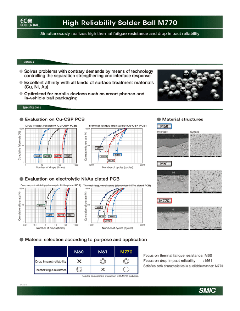
High Reliability Solder Ball M770 Simultaneously realizes high thermal fatigue resistance and drop impact reliability Features ● Solves problems with contrary demands by means of technology controlling the separation strengthening and interface response ● Excellent affinity with all kinds of surface treatment materials (Cu, Ni, Au) ● Optimized for mobile devices such as smart phones and in-vehicle ball packaging Specifications ● Evaluation on Cu-OSP PCB Drop impact reliability (Cu-OSP PCB) Thermal fatigue resistance (Cu-OSP PCB) 99.9 Cumulative failure rate (%) Cumulative failure rate (%) 99.9 M60 Interface Surface Ni 10 10 M60 1 ● Material structures 1 M705 M770 10 M61 100 M60 M705 M770 1 1000 1000 Number of drops (times) M61 Number of cycles (cycles) 10000 M61 Ni ● Evaluation on electrolytic Ni/Au plated PCB Drop impact reliability (electrolytic Ni/Au plated PCB) Thermal fatigue resistance (electrolytic Ni/Au plated PCB) 99.9 10 Cumulative failure rate (%) Cumulative failure rate (%) 99.9 M60 M770 M61 1 0.01 M770 10 M705 1 10 100 Number of drops (times) 1000 Ni M705 1 0.1 M61 1000 M60 M770 Number of cycles (cycles) 10000 ● Material selection according to purpose and application Drop impact reliability Thermal fatigue resistance M60 M61 M770 × ◎ ◎ ○ ◎ × Results from relative evaluation with M705 as basis. JPCA13-02 Focus on thermal fatigue resistance: M60 Focus on drop impact reliability : M61 Satisfies both characteristics in a reliable manner: M770 M705-RGS800HF T5 Type 5 powder realizes packaging of microscopic components Features ● Our original fine powder and flux ensure good printability ● Stable printability suppresses fusion defects at BGA joints ● Halogen-free, which suppresses fusion defects at BGA joints even with air reflow Specifications ● Excellent printability for fine patterns ensured ● Type5 has a high filling rate, ensuring proper soldering Type4 【Φ250μm】 Type4 μ Type4 solder powder Type5 Type5 solder powder Type5 【250×250μm】 Type4 φ20~38μm Type5 φ15~25μm ● Short circuiting of narrow-pitch patterns is suppressed ● Air reflow is possible and fusion defects are suppressed Conventional Type4 paste RGS800HF Type5 paste Type5 with conventional halogen-free flux Type 5 using RGS800HF ● Stable printability preventing fusion defects caused by insufficient solder amount ■ Type5 with conventional halogen-free flux Solder paste Flux BGA Solder ball Oxide film BGA ① PWB Printing/Mounting ■ Type5 using RGS800HF PWB PWB Reflow BGA Printing/Mounting Joint BGA ③ PWB ② BGA RGS800HF Solder paste JPCA13-01 Fusion failure BGA PWB Reflow PWB ③ Joint ③ ① If the solder amount is insufficient, the oxide film removal effectiveness of the flux becomes weak, resulting in fusion defects. ② Conventional halogen-free flux has weak oxide film removal ability, so it is easy for fusion defects to form. ③ Good halogen-free flux with a uniform amount of solder allows for the oxide film to be removed for all balls, so there are not fusion defects. NSV320 Transfer paste for 3D PoP (Package of Package) packaging NSV320 Features ● Possesses excellent transferability and significantly reduces contact non-wet failures in ball-to-ball stacking ● Accommodates PoP and TMV packaging and realizes excellent solderability ● Robust against warping, achieves higher performance than that of conventional products while being halogen-free Specifications ● NSV320 provides excellent solder transfer in specific amounts Insufficient solder amount Print Transfer1 Transfer2 Transfer3 Mount Joint Mount Joint Solder printing paste lacking transferability Sufficient solder amount Print Transfer1 Transfer2 Transfer3 ● PoP Packaging using NSV320 Conventional product NSV320 with excellent transferability Contact non-wet past Contact non-wet failures are observed Contact non-wet past Contact non-wet past NSV320 Contact non-wet failures are ignificantly reduced ● Stable transcript level after dwell time of 300ms or more 5 dwell time 50ms Weight(mg) 4.5 4 3.5 3 2.5 2 0 100 200 300 400 500 600 700 Dwell time(ms) JPCA13-03 800 900 1000 dwell time 300ms dwell time 999ms S101-S4-HF Solves “Non-Wet Open (NWO)”, a new non-wet type BGA solder joint defect Features ● Optimal alloy and flux were developed by understanding the NWO mechanism ● Resolves NWO defects with surface treatment materials for Cu-OSP boards, etc. ● Resolved by developing a material without changing the reflow profile Specifications ● Thin BGA packages cause large, complicated warping at low temperatures Shorter larger Example of thin BGA warpage during heating ● Difference in fusion defect mode between “HIP and “NWO” Defect mode differs according to differences in warpage behavior during preheating and the adhesion status. HIP(Head in pillow) HIP(Head in pillow) Board warpage (Type A) BGA BGA BGA BGA Fusion defect BGA Flux Powder PCB PCB Occurs when the BGA solder bump and solder paste become detached during preheating PCB Printing NWO(No wet open) PCB Mounting NWO(No wet open) BGA BGA BGA PCB Printing PCB Mounting ● Photos showing pealed surface with “HIP” and “NWO” 【BGA side】 JPCA13-04 【PCB side】 Head in pillow Head in pillow No wet open No wet open Fusion defect BGA Flux Powder Flux Powder PCB Fusion Board warpage (Type B) BGA Occurs when the board electrode and solder paste become detached during preheating PCB Reflow PCB Reflow PCB Fusion ● NWO defect improvement Photos of “NWO” NWO(No wet open) Cross-section Good joint X-ray Confirmed that NWO defects were improved compared to conventional products when using the developed S101HF(N) M53 M53 series solder paste that is capable of being applied to small-sized and lightweight on-board products Features ● Exhibits superior thermal fatigue resistance and maintains high bond strength even under severe environments ● Prevents crack propagation due to thermal fatigue and maintains electrical conductivity after long term use ● Ensures high quality even in products with small-sized and lightweight designs having small land areas Specifications ● Comparison of thermal fatigue resistance using a chip resistor ● Comparison of thermal fatigue resistance using a chip capacitor Using a 3216 chip resistor and a large-sized pattern 90 Shear strength (N) Shear strength (N) 60.0 70 M53 60 50 40 30 20 SAC305 10 0 Using a 3216 chip resistor and a medium-sized pattern 70.0 80 0 500 1000 1500 2000 2500 3000 Temperature cycle (cyc.) 3500 50.0 M53 40.0 30.0 20.0 SAC305 10.0 4000 4500 0 0 500 1000 1500 2000 Temperature cycle (cyc.) TCT;-40/+124℃(30min) M53 containing Bi and In exhibits a much lower decrease in strength compared to SAC305 2500 3000 3500 TCT;-40/+124℃(30min) M53 containing Bi and In maintains superior shear strength compared to SAC305 ● Ensures strength even on a small surface 90.0 80.0 Using a 3216 chip resistor and small-, medium- and large-sized patterns M53 In Shear strength (N) 70.0 60.0 M53 3000cyc. 50.0 40.0 SAC305 In 30.0 20.0 10.0 0.0 35 SAC305 3000cyc. L M 3 25 S 2 Surface area (mm2) 15 1 TCT;-40/+125℃ (30min) ● Comparison of cross sectional photographs SAC305 M53 Initial stage Solder alloy with greater strength and stress relaxation properties 3000cyc Initial stage Temperature cycle Temperature cycle Chip Chip Crack has grown during soldering JPCA13-05 3000cyc Larger structure compared to that of SAC305 Chip Chip No cracks MACROS "MACROS" that prevents migration Features ● No cracking of flux residue occurs even under environment with rapid temperature changes, such as in on-board equipment ● Flux residue with high adhesiveness and water repellency prevents the occurrence of migration ● Excellent for laser soldering, prevents flux spattering peculiar to laser soldering Specifications ● Cracks on flux become the cause of migration Water passage in cracks Migration Flux residue Cracks or breaking occur or breakage Dew Voltage Temperature condensation application cycle Ion migration Crack Flux residue Water Migration Solder Occurrence of cracks or breakage Soldering Water passage is formed in cracks or breakage ● Prevents the occurrence of cracks Short circuit due to migration in flux residue during temperature cycle tests JIS Grade A product MACROS When condensed water remains, ion migration easily occurs. ● Water drop test result after temperature cycle JIS Grade A product MACROS Ion migration occurs at cracks No cracks or ion migration occur Cracks No cracks Ion migration Crack Water drop test 5 V of voltage applied Temperature cycle test ; -30℃/110℃ 2000cyc. ● Provides good break-off, ensuring good drag soldering 1.00E+14 Insulation resistance [Ω] MACROS Conventional product MACROS Migration occurs in a short period of time because water penetrates easily Migration does not occur because water does not penetrate easily Conventional product 1.00E+12 Substrate only (Blank) 1.00E+10 MACROS 1.00E+08 Conventional product 1.00E+06 1.00E+04 JPCA13-06 0 2 4 Time [h] 6 8 10 ● Comparison of flux scattering in laser soldering [Test condition] Temperature: 121°C Humidity: 100% RH Atmospheric pressure: 2 atm Applied voltage: 50 V Measuring voltage: 100 V Measurement time: every 0.5 h Applied voltage mode: DC Flux scattering is prevented by viscosity suppression Solder Paste Containing Ni Balls Achieves excellent heat dissipation characteristics in horizontal packaging that suppresses void formation Features ● Suppresses cracks related to solder thickness and angle, excellent heat dissipation packaging ● Highly reliable wire bonding possible for flat bare chips ● Suppresses voids by optimal formulation of uniform Ni balls using our original technology Specifications ● Resolves issues related to power device packaging ● Achieves horizontal packaging using Semiconductor Solder Insulated board Heat sink Resolves issues related to power device packaging Uniform thickness Void reduction solder paste with Ni balls Normal solder paste may cause the chip to become tilted DIE DIE Powder High-quality alloy DIE PCB PCB PCB Printing Mounting Fusion Solder paste with Ni allows for horizontal packaging by spacers Cracks occur at thin portions during the cooling cycle Uniform Ni ball development Increased voids ↓ Selection of a solder alloy that Resistance and can endure sever conditions Powder heat dissipation decrease Ni ball Original paste development DIE DIE PCB Development of various alloys according to usage DIE PCB PCB Printing Mounting Fusion ● Uniform Ni balls based on our original technology allow for excellent heat dissipation ●Without Ni ball Air in cracks disrupt heat conductivity and decrease heat dissipation Bare chip Cracks caused by tilting Chip is tilted and the solder thickness is uneven ●With Ni ball Chip Ni ball Preform Cracks caused by thin solder Good heat dissipation Ni Ball Solder Board Ni balls ensure parts standoff 200 ● Optimal formulation of Ni balls Void images With Without Solder thickness [um] 150 suppresses void formation Spacer Ni balls suppress uneven solder thickness 100 50 0 A B C D With Ni balls E A B C D E Without Ni balls Results of solder thickness at each measurement point JPCA13-07 M705-NX001 Increases fluidity of solder in a melted state to eliminate voids Features ● Good wettability increases the fluidity of heated solder ● Good wettability even with Cu-OSP boards, voids are suppressed ● Excellent insulation reliability while maintaining good wettability Specifications ● Voids are bad because they disrupt ● Void formation mechanism heat dissipation Terminals such as LGAs and dies with few openings have many voids Cu-OSP products with poor wettability have many voids Void Paste Mounting Au-plated product Sufficient wetting is ensured at the Cu base material lead cross-section where soldering is difficult Conventional Product Void Solidification Fusion The better the wettability, the better the fluidity Cu-OSP product ● Excellent wettability Solder flow ● Voids are greatly reduced by the optimal profile of the fusion temperature range and NX001 Conventional Product Au-platted product N705-NX001 Cu-OSP product Cu-OSP product Power transistor M705-NX001 QFN bottom electrode Voids are greatly reduced even for Cu-OSP boards ● Excellent insulation reliability maintained while ensuring good wettability Recommended optimal profile 85℃ 85% RH1000hr Applied Voltage 45V 1.E+10 At 220℃: 40 to 60 Sec. 250 1.E+09 1.E+07 Temperature [℃] Resistance [Ω] 1.E+08 1.E+06 1.E+05 1.E+04 1.E+03 1.E+02 1.E+01 1.E+00 JPCA13-08 0 200 400 600 Elapsed time [hr] 800 1000 200 150 100 50 0 0 50 100 Time [sec] 150 200 250


