28GHz Frequency Divider FD28B FD28B
advertisement
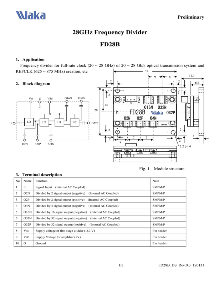
Preliminary 28GHz Frequency Divider FD28B 1. Application Frequency divider for full-rate clock (20 ~ 28 GHz) of 20 ~ 28 Gb/s optical transmission system and 37 REFCLK (625 ~ 875 MHz) creation, etc 9 2 2. Block diagram 2 O32N O16N Vdd G G 14 28 O16N U FD28B In 1/2 1/4 1/2 O32N CNO32P U U U O2N11 1/2 In 3 2 O2P O4N 7 O32P FD28B 2 2 7 2 O2N O2P 6.6 2 2 Vss 11.1 8 3 7 2 8 O4N 2.2φ- 4 Fig. 1 Module structure 3. Terminal description No Name Function Note 1 In Signal Input 2 O2N Divided by 2 signal output (negative) (Internal AC Coupled) SMPM/P 3 O2P Divided by 2 signal output (positive) (Internal AC Coupled) SMPM/P 4 O4N Divided by 4 signal output (negative) (Internal AC Coupled) SMPM/P 5 O16N Divided by 16 signal output (negative) (Internal AC Coupled) SMPM/P 6 O32N Divided by 32 signal output (negative) (Internal AC Coupled) SMPM/P 7 O32P Divided by 32 signal output (positive) (Internal AC Coupled) SMPM/P 8 Vss Supply voltage of first stage divider (-3.3 V) Pin header 9 Vdd Supply Voltage for amplifier (5V) Pin header 10 G Ground Pin header (Internal AC Coupled) SMPM/P 1/3 FD28B_DS Rev.0.3 120131 Preliminary 4. Absolute maximum ratings Terminal Parameter Symbol Unit Min Max Vss Supply voltage of first stage divider Vss V -3.7 0.5 Vdd Supply Voltage for amplifier Vdd V 5.5 In Applied input power Pin Vpp 1.0 (+4 dBm) ESD tolerance (HBM) Vesd V -TBD +TBD Storage temperature Tst Degree C -40 80 5. Characteristics (Ta=25 [℃]) Related Parameter Symbol Unit terminal Min In Input frequency GHz 2< fin <6 GHz PminL dBm -7 (0.28Vpp) fin > 6GHz PminH dBm -20 (0.062Vpp) Pmax dBm + 3 (0.89Vpp) RLin dB > 9 Divided by 2 output frequency fout2 GHz Output power (single ended) PO2 dBm -9 (0.23Vpp) Rise/fall time (20-80 %) tr/tf2 ps 12/14 ps Divided by 4 output frequency fout4 GHz Output power (single ended) PO4 dBm -7 (0.28Vpp) Rise/fall time (20-80 %) tr/tf4 ps 17/16 ps Divided by 16output frequency fout16 GHz Output power (single ended) PO16 dBm -4 (0.4Vpp) Rise/fall time (20-80 %) tr/tf16 ps 100 ps Divided by 32 output frequency fout32 GHz Output power (single ended) PO32 dBm +3.1 (0.9Vpp) Rise/fall time (20-80 %) tr/tf32 ps 100 ps Supply voltage of first stage divider Vss V Supply current of Vss Iss mA Supply voltage of dividers except first divider Vdd V Supply Current of Vdd Idd mA 340 Power dissipation Pdiss W 2.4 Maximum Input power Input return loss O2N, O2P O4N O16N O32N,O32P Vdd Vss,Vdd Typ fin Minimum Input power Vss Specification fout < 20 GHz 3.2 28 1.6 14 0.8 7 0.2 1.75 0.1 -3.5 Max 0.875 -3.3 -3.1 210 4.75 5 5.25 6. Precaution This product uses ESD sensitive high-speed devices. Handle it with appropriate precaution described below. 1) Connect the ground (G) terminal of FD28B to the highest quality ground line in the room and connect this terminal to the ground terminal of test equipment as well. 2) Use ESD protection wrist strap which is connected to FD28B ground. 2/3 FD28B_DS Rev.0.3 120131 Preliminary 3) Avoid abnormal mechanical shock. 7. Attachment 1) 30 cm Jumper cable with pin header socket: 1 3/3 FD28B_DS Rev.0.3 120131


