MT test W09
advertisement
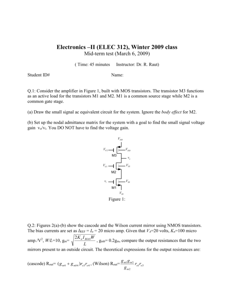
Electronics –II (ELEC 312), Winter 2009 class Mid-term test (March 6, 2009) ( Time: 45 minutes Student ID# Instructor: Dr. R. Raut) Name: Q.1: Consider the amplifier in Figure 1, built with MOS transistors. The transistor M3 functions as an active load for the transistors M1 and M2. M1 is a common source stage while M2 is a common gate stage. (a) Draw the small signal ac equivalent circuit for the system. Ignore the body effect for M2. (b) Set up the nodal admittance matrix for the system with a goal to find the small signal voltage gain vo/vi. You DO NOT have to find the voltage gain. VDD VG 2 VDD M3 vo VSS VG1 M2 vi VSS M1 VSS Figure 1: Q.2: Figures 2(a)-(b) show the cascode and the Wilson current mirror using NMOS transistors. The bias currents are set as IREF = Io = 20 micro amp. Given that VA=20 volts, Kn=100 micro 2 K n I BIASW amp./V2, W/L=10, gm= , gmb= 0.2gm, compare the output resistances that the two L mirrors present to an outside circuit. The theoretical expressions for the output resistances are: (cascode) Rout= ( g m 4 g mb4 )ro3 ro 4 , (Wilson) Rout= g m1 g m3 ro1ro3 g m2 Q.3 The BJT differential amplifier is supplied with a differential ac signal vD= v1-v2. The differential output signal is given by the expression exp( v D / VT ) exp( v D / VT ) vo1 vo 2 Rc I [ ] 1 exp( v D / VT ) 1 exp( v D / VT ) Where VT is the thermal voltage (~ 25 mV). The bias current I is arranged to be 2 mA Determine the voltage gain (vo1-v02)/vD, when (i) vD=20 mV and (ii) vD= 2 mV. How do these compare with the theoretical small signal voltage gain value of | gmRC|, where gm is the transconductance of each BJT device. 10V 2 k v1 vo2 vo1 vD v 2 I 10V Figure 3 re / gm BJTs h fe h fe 1 Diodes ****** Some useful formulae********** gm IC /VT r h fe / gm h fe ic / ib ro VA / I C VT kT 25mV at room temperature q I=Is exp(vBE/VT)

