MMQ60R070P - MagnaChip
advertisement
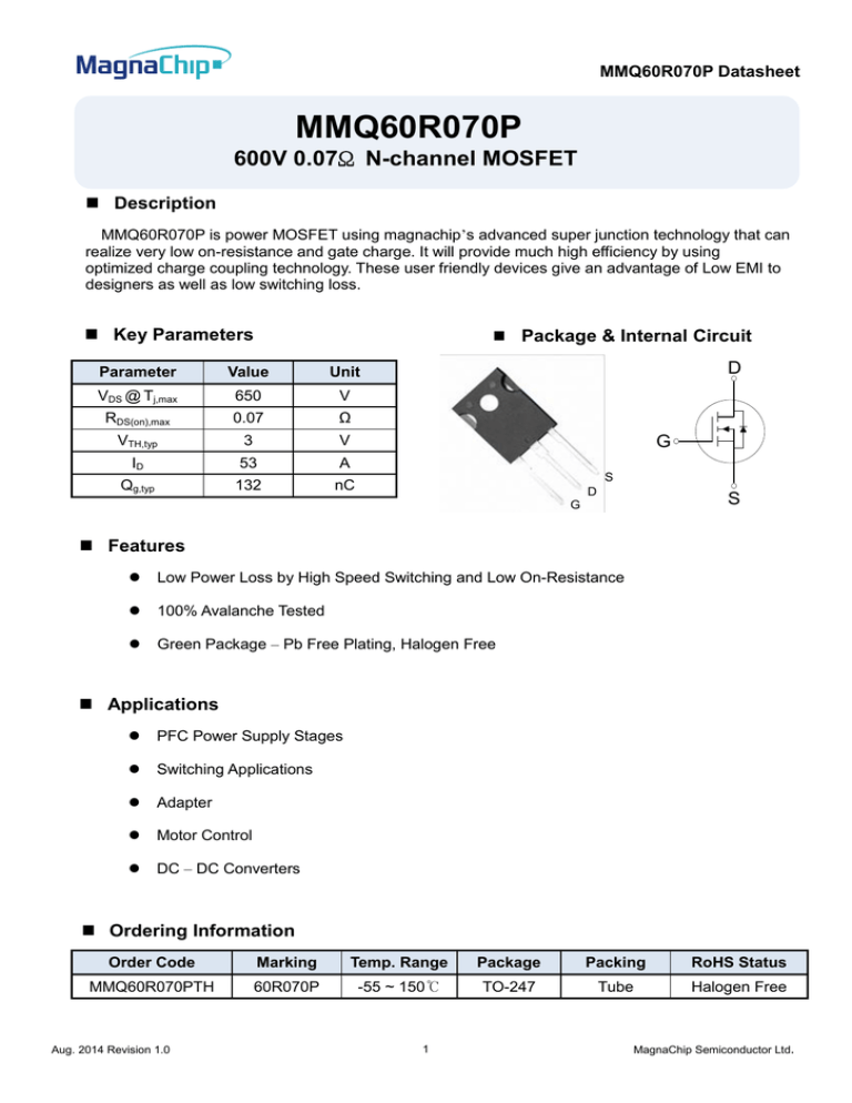
MMQ60R070P Datasheet MMQ60R070P 600V 0.07Ω N-channel MOSFET Description MMQ60R070P is power MOSFET using magnachip’s advanced super junction technology that can realize very low on-resistance and gate charge. It will provide much high efficiency by using optimized charge coupling technology. These user friendly devices give an advantage of Low EMI to designers as well as low switching loss. Key Parameters Package & Internal Circuit Parameter Value Unit VDS @ Tj,max 650 V RDS(on),max 0.07 Ω VTH,typ 3 V ID 53 A Qg,typ 132 nC D G S D G G G S Features Low Power Loss by High Speed Switching and Low On-Resistance 100% Avalanche Tested Green Package – Pb Free Plating, Halogen Free Applications PFC Power Supply Stages Switching Applications Adapter Motor Control DC – DC Converters Ordering Information Order Code Marking Temp. Range Package Packing RoHS Status MMQ60R070PTH 60R070P -55 ~ 150℃ TO-247 Tube Halogen Free Aug. 2014 Revision 1.0 1 MagnaChip Semiconductor Ltd. MMQ60R070P Datasheet Absolute Maximum Rating (Tc=25℃ unless otherwise specified) Parameter Symbol Rating Unit Drain – Source voltage VDSS 600 V Gate – Source voltage VGSS ±30 V 53 A TC=25℃ 33.5 A TC=100℃ Continuous drain current ID Pulsed drain current(1) IDM 159 A Power dissipation PD 391 W Single - pulse avalanche energy EAS 1135 mJ MOSFET dv/dt ruggedness dv/dt 50 V/ns Diode dv/dt ruggedness dv/dt 15 V/ns Tstg -55 ~150 ℃ Tj 150 ℃ Storage temperature Maximum operating junction temperature 1) 2) Note Pulse width tP limited by Tj,max ISD ≤ ID, VDS peak ≤ V(BR)DSS Thermal Characteristics Parameter Symbol Value Unit Thermal resistance, junction-case max Rthjc 0.32 ℃/W Thermal resistance, junction-ambient max Rthja 62.5 ℃/W Aug. 2014 Revision 1.0 2 MagnaChip Semiconductor Ltd. MMQ60R070P Datasheet Static Characteristics (Tc=25℃ unless otherwise specified) Parameter Symbol Min. Typ. Max. Unit Drain – Source Breakdown voltage V(BR)DSS 600 - - V VGS = 0V, ID=0.25mA VGS(th) 2 3 4 V VDS = VGS, ID=0.25mA Zero Gate Voltage Drain Current IDSS - - 1 μA VDS = 600V, VGS = 0V Gate Leakage Current IGSS - - 100 nA VGS = ±30V, RDS(ON) - 0.063 0.07 Ω VGS = 10V, ID = 25.8A Gate Threshold Voltage Drain-Source On State Resistance Test Condition VDS =0V Dynamic Characteristics (Tc=25℃ unless otherwise specified) Parameter Symbol Min. Typ. Max. Input Capacitance Ciss - 4440 - Output Capacitance Coss - 2965 - Unit pF Reverse Transfer Capacitance Crss - 165 - Effective Output Capacitance Energy Related (3) Co(er) - 112 - Turn On Delay Time td(on) - 70 - tr - 200 - Rise Time Turn Off Delay Time td(off) - 410 - tf - 162 - Total Gate Charge Qg - 132 - Gate – Source Charge Qgs - 31 - Gate – Drain Charge Qgd - 58 - Gate Resistance RG - 2.4 - Fall Time Test Condition VDS = 25V, VGS = 0V, f = 1.0MHz VDS = 0V to 480V, VGS = 0V,f = 1.0MHz ns VGS = 10V, RG = 25Ω, VDS = 300V, ID = 53 A nC VGS = 10V, VDS = 480V, ID = 53 A Ω VGS = 0V, f = 1.0MHz 3) Co(er) is a capacitance that gives the same stored energy as COSS while VDS is rising from 0V to 80% V(BR)DSS Aug. 2014 Revision 1.0 3 MagnaChip Semiconductor Ltd. MMQ60R070P Datasheet Reverse Diode Characteristics (Tc=25℃ unless otherwise specified) Parameter Symbol Min. Typ. Max. Unit Continuous Diode Forward Current ISD - - 53 A Diode Forward Voltage VSD - - 1.4 V Reverse Recovery Time trr - 582 - ns Reverse Recovery Charge Qrr - 13.7 - μC Reverse Recovery Current Irrm - 47 - A Aug. 2014 Revision 1.0 4 Test Condition ISD = 53.0 A, VGS = 0 V ISD = 53.0A di/dt = 100 A/μs VDD = 100 V MagnaChip Semiconductor Ltd. MMQ60R070P Datasheet Aug. 2014 Revision 1.0 5 MagnaChip Semiconductor Ltd. MMQ60R070P Datasheet Aug. 2014 Revision 1.0 6 MagnaChip Semiconductor Ltd. MMQ60R070P Datasheet Aug. 2014 Revision 1.0 7 MagnaChip Semiconductor Ltd. MMQ60R070P Datasheet Test Circuit Same type as DUT VGS Qg 100KΩ 10V 10V + Qgs VDS Qgd 1mA DUT 10V Charge Fig15-2. Gate charge waveform Fig15-1. Gate charge measurement circuit trr DUT IFM IF 0.5 IRM + V - DS IS tb 0.25 IRM di/dt L Rg 10KΩ ta 0.75 IRM IRM + Same type as DUT VDD VR Vgs ± 15V VRM(REC) Fig16-1. Diode reverse recovery test circuit Fig16-1. Diode reverse recovery test waveform ID DUT VDS VDS Rg 25Ω 90% RL Vgs 10% tp + VDD VGS - Td(on) tr Td(off) ton Fig17-1. Switching time test circuit for resistive load tf toff Fig17-2. Switching time waveform IAS DUT VDS BVDSS tp Rg L Vgs tAV IAS VDD tp VDS(t) + VDD Rds(on) * IAS Fig18-1. Unclamped inductive load test circuit Aug. 2014 Revision 1.0 Fig18-2. Unclamped inductive waveform 8 MagnaChip Semiconductor Ltd. MMQ60R070P Datasheet Physical Dimension TO-247 E ΦP Dimensions are in millimeters, unless otherwise specified A L1 D E2 D1 S Q A2 b2 L b1 b E1 c e Dimension Min(mm) Max(mm) A 4.70 5.31 A1 2.20 2.60 A2 1.50 2.49 b 0.99 1.40 b1 2.59 3.43 b2 1.65 2.39 c 0.38 0.89 D 20.30 21.46 D1 13.08 - E 15.45 16.26 E1 13.06 14.02 E2 4.32 5.49 e L 5.45BSC 19.81 20.57 L1 - 4.50 ΦP 3.50 3.70 Q 5.38 S Aug. 2014 Revision 1.0 A1 6.20 6.15BSC 9 MagnaChip Semiconductor Ltd. MMQ60R070P Datasheet DISCLAIMER: The Products are not designed for use in hostile environments, including, without limitation, aircraft, nuclear power generation, medical appliances, and devices or systems in which malfunction of any Product can reasonably be expected to result in a personal injury. Seller’s customers using or selling Seller’s products for use in such applications do so at their own risk and agree to fully defend and indemnify Seller. MagnaChip reserves the right to change the specifications and circuitry without notice at any time. MagnaChip does not consider responsibility for use of any circuitry other than circuitry entirely included in a MagnaChip product. is a registered trademark of MagnaChip Semiconductor Ltd. Aug. 2014 Revision 1.0 10 MagnaChip Semiconductor Ltd.
