APPLICATION NOTE
M16C/62
Using the M16C/62 D-A Converter
1.0 Abstract
The following article introduces and shows an example of how to use the D-A Converter on the M16C/62 group
device.
2.0 Introduction
The Renesas M16C/62 series of microcontrollers is a 16-bit family of MCUs, based on Renesas’ popular M16C
CPU core. These parts provide high memory efficiency, power-saving ability, low noise emission, and improved
noise immunity. The M16C family features an impressive list of features including LCD, USB,
10-bit A-D converter, UARTs, timers, DMA controllers, D-A converter, and large on-chip ROM and RAM and
FLASH. The M16C/62 part series can be used in many applications such as office equipment, PC peripherals,
portable devices, automotive, cameras, audio, and more.
This article shows how to create a simple waveform generator using the D-A converter and other peripherals on
the M16C/62 series of microcontrollers.
3.0 D-A Converter
Digital-to-Analog conversion is a process in which digital signals are converted into analog signals. The circuit
that performs this function is the D-A converter (DAC). Some common examples of DAC uses are for modems,
motor control, and audio output.
The M16C/62 group microcontroller contains two independent 8-bit D-A converter channels. This D-A converter
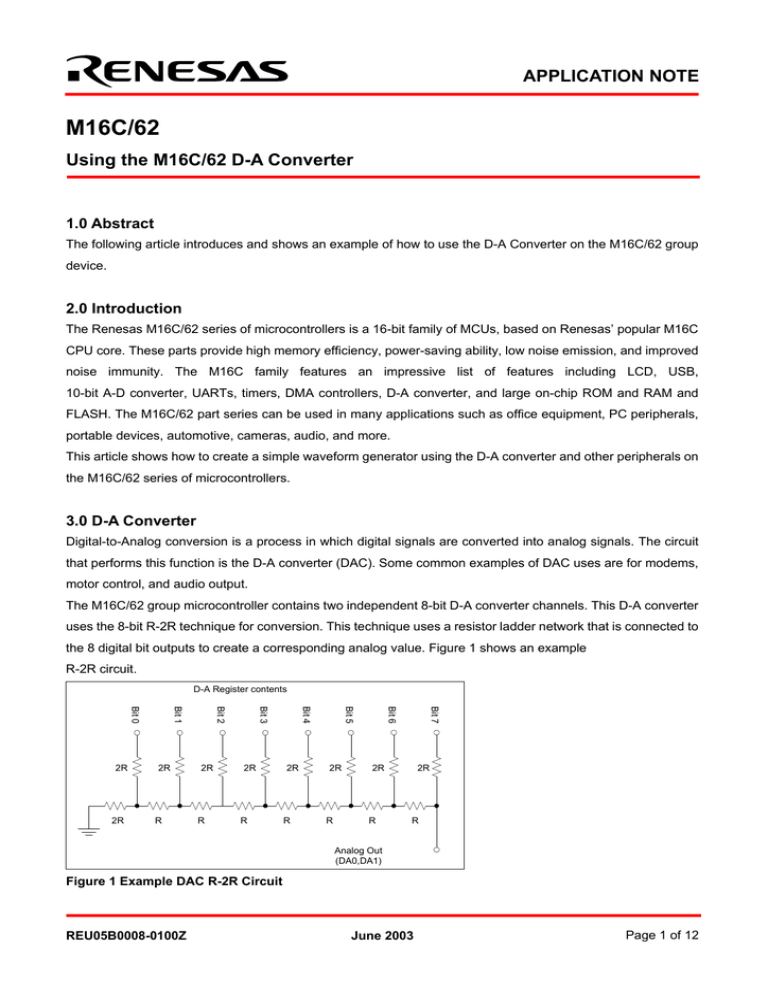
uses the 8-bit R-2R technique for conversion. This technique uses a resistor ladder network that is connected to
the 8 digital bit outputs to create a corresponding analog value. Figure 1 shows an example
R-2R circuit.
D-A Register contents
R
Bit 7
R
2R
Bit 6
R
2R
Bit 5
R
2R
Bit 4
R
2R
Bit 3
2R
Bit 2
2R
Bit 1
Bit 0
2R
2R
R
2R
R
Analog Out
(DA0,DA1)
Figure 1 Example DAC R-2R Circuit
REU05B0008-0100Z
June 2003
Page 1 of 12
M16C/62
Using the M16C/62 D-A Converter
The analog output voltage of the DAC has a total range from 0V to VREF. The output voltage can be calculated
at any time by using
DAC Output = (VREF/256) x D-A register contents
The following is a list of all the DAC related pins and registers in the M16C/62:
D-A converter related pins:
• DA0 pin – Analog output of D-A channel 0
• DA1 pin – Analog output of D-A channel 1
• VREF – External reference voltage
• Avcc, Avss – Power and ground pins used by the DAC
D-A converter related registers:
• D-A Register 0 (DA0) – Digital value for D-A conversion, output on channel 0
• D-A Register 1 (DA1) – Digital value for D-A conversion, output on channel 1
• D-A Control Register (DACON) – D-A enable bits (refer to Figure 2)
• Port 9 Direction Register (PD9) – Set DA0 pin and DA1 pin to outputs
D-A control register
b7
b6
b5
b4
b3
b2
b1
Symbol
DACON
b0
Address
03DC16
Bit symbol
When reset
0016
Bit name
Function
DA0E
D-A0 output enable bit
0 : Output disabled
1 : Output enabled
DA1E
D-A1 output enable bit
0 : Output disabled
1 : Output enabled
RW
Nothing is assigned.
In an attempt to write to these bits, write “0”. The value, if read, turns out to be “0”
D-A register
b7
Symbol
DAi (i = 0,1)
b0
Address
03D816, 03DA16
When reset
Indeterminate
Function
RW
R
W
Output value of D-A conversion
(JB-02-UM60)
Figure 2 D-A Control and Data Registers for M16C/62
To perform a D-A conversion:
1. Set the D-A channel output pin(s) that will be used for output mode in the Port 9 Direction Register.
2. Write the initial value to be converted to the D-A register (DA0, DA1). D-A conversion starts when a value is
written to the D-A register.
3. Set the D-A output enable bit to “1” to start outputting the analog signal on the DA pin.
REU05B0008-0100Z
June 2003
Page 2 of 12
M16C/62
Using the M16C/62 D-A Converter
4. Write new digital values to the D-A register at any time to be converted and sent out on the DA pin.
5. The D-A converter continues outputting an analog signal until the D-A output is disabled by setting the D-A
enable bit to “0”.
More information on the D-A converter can be found in the M16C/62 group data sheet.
4.0 Implementation
A simple waveform generator sample program is included to demonstrate the use of the D-A converter. This
program is written to run on Renesas’ MSV1632 evaluation board. This board allows easy evaluation for any
M16C/62 microcontroller. More information on this evaluation board and other starter kits can be found at
http://www.renesaschips.com.
4.1 Program Operation
This program generates a square wave, a triangle wave, or a sine wave and outputs it on D-A channel 0 (DA0
pin). The frequency and amplitude of any of the waveforms are adjustable using the push buttons on the
evaluation board, except that the amplitude for the sine wave cannot be changed. The amplitude of the sine
wave is fixed to 5 volts, where the maximum amplitude of the square and triangle waveforms can be changed
from 0 to 5 volts. The frequency for any of the waveforms can be changed from approximately 30 Hz to 800 Hz.
Connect an oscilloscope to the DA0 pin to see the output waveforms.
There are three push buttons on the evaluation board that are used to change the waveform type, the frequency,
and the amplitude. The button labeled SW1 is used for a mode select function. Pushing this button changes the
mode to one of the following: Waveform Type, Amplitude, or Frequency. The current selected mode is displayed
on the LCD. The buttons SW2 and SW3 are used to modify the values of the current selected mode. Pushing
SW2 causes the waveform type to cycle forwards, the amplitude to increase in value, and the frequency to
increase. Pushing SW3 causes the waveform type to cycle backwards, the amplitude to decrease, and the
frequency to decrease. When an amplitude or frequency reaches its maximum or minimum value, a message is
displayed on the LCD indicating max or min.
4.2 Triangle Waveform
The triangle waveform is a good example of how the D-A converter works. Start by putting 0 into the D-A register.
Now for every step of the waveform just add 1 to the value that was previously written to the D-A register. By
stepping up from 0016 to FF16 in the D-A register, a rising line is created that goes from 0 volts to 5 volts (or
VREF voltage) with its slope dependent on the amount of time between steps. Once FF16 is reached, the
program starts subtracting 1 from the D-A register every step. This will create a downward sloped line. When
0016 is reached, the process is repeated. Continue to repeat this procedure to create a continuous triangle wave.
Adding or subtracting 1 from the D-A register produces the highest resolution waveform. If less resolution is
desired, divide the desired resolution by 255 and add or subtract this number from the D- A register for every
step.
REU05B0008-0100Z
June 2003
Page 3 of 12
M16C/62
Using the M16C/62 D-A Converter
In the sample program included, the D-A register is changed by 2 for every step. This produces a full cycle in 256
steps.
Figure 3 Triangle Wave Output
4.3 Square Waveform
The square wave is also easy to produce with the D-A converter. Basically setting the D-A register to 0016 will
produce the “low” (0V) portion of the waveform, and setting the D-A register to FF16 will produce the “high”
(VREF) portion of the waveform.
In order to keep the frequency between waveforms the same in the sample program, the square wave only
changes states every 128 steps. This produces a full cycle in 256 steps.
Figure 4 Square Wave Output
4.4 Sine Waveform
The easiest way to create a sine wave is by using a lookup table of predefined sine values. For every step of the
sine wave, the next value is taken from the lookup table and put into the D-A register. When the last value is
loaded, start over at the top of the table. The number of values in the lookup table is determined by the resolution
REU05B0008-0100Z
June 2003
Page 4 of 12
M16C/62
Using the M16C/62 D-A Converter
of the sine wave that is desired.
In the sample program a lookup table of 256 values is used, which is the highest resolution possible. This also
makes the sine wave consistent with the other waveforms in this sample for frequency. One cycle takes
256 steps.
Figure 5 Sine Wave Output
4.5 Frequency Adjustment
The frequency of each waveform is determined by the time interval between steps. A timer interrupt is used to
determine this time interval. Every time the timer runs out, an interrupt is generated and the next step in the
waveform is put into the D-A register.
The frequency in the sample program can be adjusted by using the SW2 and SW3 push buttons. Initially the
timer is preloaded with 7F16. When in the frequency mode, pushing SW2 will delete 2 from the timer reload
register thus causing the timer interrupts to occur more often. This creates a higher frequency waveform.
Pushing SW3 in the frequency mode subtracts 2 from the timer reload register thus causing the frequency to
slow down.
4.6 Amplitude Adjustment
The amplitude of the waveforms can be adjusted in software by limiting the maximum value put into the D-A
register. In a 5 volt system if the maximum amplitude desired is 2.5 volts, then the highest value to put into the
D-A register would be 7F16 (FF16 / 2).
The amplitude in the sample program can be adjusted on the square and triangle waves by using the SW2 and
SW3 push buttons. Since the sine wave uses a lookup table method, the amplitude of this waveform cannot be
adjusted without creating a new table. A software variable is used to store the current maximum amplitude
setting. The max amplitude setting is initialized to FF16. When in the frequency mode, pushing SW2 will add 2 to
the max amplitude setting causing the amplitude to increase. Pushing the SW3 push button will subtract 2 from
the max amplitude setting causing the amplitude to decrease.
The amplitude of the waveforms could also be controlled in hardware by using the VREF pin. The D-A converter
REU05B0008-0100Z
June 2003
Page 5 of 12
M16C/62
Using the M16C/62 D-A Converter
will always output between 0 volts and VREF.
5.0 Conclusions
The D-A feature of the M16C/62 microcontroller allows easy conversion of digital signals to analog signals
without needing any additional components. This function can be useful for many applications where there is the
need to interface digital and analog signals together in the same design.
6.0 Reference
Renesas Technology Corporation Semiconductor Home Page
http://www.renesas.com
E-mail Support
support_apl@renesas.com
Data Sheets
• M16C/62 datasheets, 62aeds.pdf
7.0 Software Code
The example program was written to run on the MSV1632 Starter Kit but could be easily modified to any user
application. The program is written in C (using the NC30 Compiler). Not all source files are included here (excludes
LCD routines and the like), just the main program showing D-A usage. Complete sample code can be downloaded
from the Renesas website or obtained from a local Renesas Rep. This is a “no frills” program developed to show the
basic usage of the D-A Converter.
REU05B0008-0100Z
June 2003
Page 6 of 12
M16C/62
Using the M16C/62 D-A Converter
/*****************************************************************************
*
*
File Name:
da_waveform.c
Content:
M16C D-A converter sample program
*
*
*
This program is a simple waveform generator that outputs
*
Triangle, Square or Sine waves with adjusted frequency and
*
amplitude.
*
This program was written to run on the MSV1632 Evaluation Board
*
*
Version: 1.10
*
Date:
09-19-2002
*
*
Copyright 2003 Renesas Technology Corporation
*
All rights reserved
*
*=============================================================================
*
$Log:$
*===========================================================================*/
#include "sfr62a.h"
/* SFR register definition */
#include "display_1632-62.h"
/* LCD display routines */
#pragma INTERRUPT ta0_isr
/* Interrupt declarations */
#pragma INTERRUPT int0_isr
#pragma INTERRUPT int1_isr
#pragma INTERRUPT int2_isr
unsigned char mode = 0;
/* variable declarations */
unsigned char amp = 0xff;
/* current amplitude */
unsigned char freq = 0x7f;
/* current frequency */
unsigned char type = 1;
/* current waveform type */
unsigned char count = 1;
/* freq delay counter */
unsigned const char banner1[] = "D to A Waveforms"; /* LCD Panel Outputs */
unsigned const char banner2[] = "<--- Use buttons";
unsigned const char mode0[] = "
Waveform";
unsigned const char mode1[] = "
Amplitude";
unsigned const char mode2[] = "
Frequency";
unsigned const char type1[] = "Square
";
unsigned const char type2[] = "Triangle";
unsigned const char type3[] = "Sine
extern const unsigned char sin_table[];
";
/* sine function lookup table */
/*****************************************************************************
Name:
main
Parameters:
None
Returns: None
Description: Initializes the system and enters the main loop
*****************************************************************************/
void main()
{
prc0 = 1;
/* Unlock the System Clock Control Register */
cm06 = 0;
/* Set the divide clock to CM16 and CM17 */
REU05B0008-0100Z
June 2003
Page 7 of 12
M16C/62
Using the M16C/62 D-A Converter
cm1 &= 0x3F;
/* Set the divide ratio to 1. */
prc0 = 0;
/* Lock the System Clock Control Register */
InitDisplay();
/* Initialize the LCD Display */
DisplayString( DISPLAY_LINE1,banner1);
/* output start-up text to LCD line 1*/
DisplayString( DISPLAY_LINE2,banner2 );
/* output start-up text to LCD line 2*/
/* Initialize Timer A0 */
ta0mr = 0x40;
/*
- timer mode, f/8 */
ta0 = 0x7f;
/*
- preload timer value */
udf = 0;
/*
- count down */
ta0ic = 0x02;
/* Set the interrupt Priority level to 2 */
int0ic = 0x03;
/* enable int0 interrupt, level 3 */
int1ic = 0x03;
/* enable int1 interrupt, level 3 */
int2ic = 0x03;
/* enable int2 interrupt, level 3 */
da0 = 0;
/* init D-A value to 0 */
da0e = 1;
/* enable d-a converter 0 */
ta0s = 1;
/* start timer A0 */
asm("FSET I");
/* enable interrupts */
while (1){
/* main loop */
asm("NOP");
/* wait for user inputs via interrupts */
}
}
/*****************************************************************************
Name:
ta0_isr
Parameters: None
Returns:
None
Description:
Timer A0 interrupt routine
This routine creates the actual waveforms.
*****************************************************************************/
void ta0_isr()
{
static unsigned char daout = 0;
/* value to be written to the d2a */
static unsigned char direction = 1;
/* current slope: inc or dec */
switch (type) {
/*********************** Square Wave ***********************/
case 1:
count +=2;
/* freq delay counter */
if (count == amp){
/* max number of delay steps? */
count = 1;
/* reset counter */
if (direction == 1) {
/* direction = up? */
daout = amp;
/* max d-a value */
direction = 0;
/* change wave direction */
daout = 0x00;
/* min d-a value */
direction = 1;
/* change wave direction */
}
else {
/* direction = down */
}
REU05B0008-0100Z
June 2003
Page 8 of 12
M16C/62
Using the M16C/62 D-A Converter
}
break;
/*********************** Triangle Wave *********************/
case 2:
if (direction == 1) {
/* direction = up? */
daout +=2;
/* add to d-a value */
if (daout >= (amp-1))
/* max amplitude? */
direction = 0;
/* change wave direction */
}
else {
/* direction = down */
daout -=2;
/* substract from d-a value */
if (daout <= 0x01)
/* min amplitude ? */
direction = 1;
/* change wave direction */
}
break;
/************************* Sine Wave ***********************/
case 3:
count++;
if (count >= 0xff)
/* max amplitude? */
count = 0;
/* reset table counter */
daout = sin_table[count];
/* get sine value from look-up table */
break;
default:
break;
}
da0 = daout;
/* output new D/A value */
}
/*****************************************************************************
Name:
int0_isr
Parameters: none
Returns:
none
Description:
INT0 interrupt routine (Switch SW1)
Pushing this switch changes the current mode
Modes: Waveform select, Amplitude adjust, Frequency adjust.
*****************************************************************************/
void int0_isr()
{
DisplayString(DISPLAY_LINE1,"
");
/* clear the LCD */
DisplayString(DISPLAY_LINE2,"
");
/* clear the LCD */
mode ++;
/* increment to next mode */
if (mode >= 3)
/* max number of modes = 3 */
mode = 0;
switch (mode) {
case 0:
DisplayString(DISPLAY_LINE1,mode0);
/* output waveform mode to LCD */
break;
REU05B0008-0100Z
June 2003
Page 9 of 12
M16C/62
Using the M16C/62 D-A Converter
case 1:
DisplayString(DISPLAY_LINE1,mode1);
/* output amplitude adj to LCD */
break;
case 2:
DisplayString(DISPLAY_LINE1,mode2);
/* output frequency adj to LCD */
break;
default:
break;
}
}
/*****************************************************************************
Name:
int1_isr
Parameters: none
Returns:
none
Description:
INT1 interrupt routine (Switch SW2)
This switch changes the waveform type, amplitude, and freq
in the upward or faster direction.
*****************************************************************************/
void int1_isr()
{
/* Clear the second line of the LCD */
DisplayString(DISPLAY_LINE2,"
if (mode == 0){
");
/* Waveform type mode */
type++;
if (type >= 4)
type = 1;
switch (type) {
case 1:
DisplayString(DISPLAY_LINE2,type1);/* output wave type to LCD*/
count = 1;
break;
case 2:
DisplayString(DISPLAY_LINE2,type2);/* output wave type to LCD*/
break;
case 3:
DisplayString(DISPLAY_LINE2,type3);/* output wave type to LCD*/
break;
default:
break;
}
}
if (mode == 1){
/* Amplitude mode */
if (amp != 0xff){
amp +=2;
/* change amplitude in 2 step increments */
DisplayString(DISPLAY_LINE2,"Up"); /* output
to LCD line 2*/
}
else DisplayString(DISPLAY_LINE2,"Max");
/* max amplitude reached */
}
if (mode == 2){
/* Frequency mode */
if (freq != 1){
REU05B0008-0100Z
/* max frequency reached? */
June 2003
Page 10 of 12
M16C/62
Using the M16C/62 D-A Converter
freq -= 2;
/* no, decrease frequency */
DisplayString(DISPLAY_LINE2,"Increase");/* output to LCD line 2*/
ta0 = freq;
/* load new value to Timer A0 */
}
else DisplayString(DISPLAY_LINE2,"Max");
/* max frequency reached */
}
}
/*****************************************************************************
Name:
int2_isr
Parameters: none
Returns:
none
Description:
INT2 interrupt routine (Switch SW3)
This switch changes the waveform type, amplitude, and freq
in the downward or slower direction.
*****************************************************************************/
void int2_isr()
{
/* Clear the second line of the LCD */
DisplayString(DISPLAY_LINE2,"
");
if (mode == 0){
/* Waveform type mode */
type--;
if (type <= 0)
type = 3;
switch (type) {
case 1:
DisplayString(DISPLAY_LINE2,type1);/* output wave type to LCD*/
count = 1;
break;
case 2:
DisplayString(DISPLAY_LINE2,type2);/* output wave type to LCD*/
break;
case 3:
DisplayString(DISPLAY_LINE2,type3);/* output wave type to LCD*/
break;
default:
break;
}
}
if (mode == 1){
/* Amplitude mode */
if (amp != 1){
amp -= 2;
/* minimum frequency reached? */
/* no, decrease amplitude */
DisplayString(DISPLAY_LINE2,"Down");
/* output
to LCD line 2*/
}
else DisplayString(DISPLAY_LINE2,"Min");
/* minimum amplitude reached */
}
REU05B0008-0100Z
June 2003
Page 11 of 12
M16C/62
Using the M16C/62 D-A Converter
if (mode == 2){
/* Frequency mode */
if (freq != 0xff){
/* frequency at minimum ? */
freq +=2;
/* no, decrease frequency */
DisplayString(DISPLAY_LINE2,"Decrease");
/* output
ta0 = freq;
/* load new value to Timer A0 */
to LCD line 2*/
}
else DisplayString(DISPLAY_LINE2,"Min");
/* Minimum frequency reached */
}
}
/*****************************************************************************
*
*
File Name:
sin.c
*
*
Content: Sine function look-up table for M16C
*
This produces a sine wave that varies from 0v to Vcc
*
using 256 steps.
Values are ready to send to D/A converter.
*
*
Version:
Rev 1.0
04/25/2002
*
*
Copyright 2003 Renesas Technology Corporation
*
All rights reserved
*
*=============================================================================
const unsigned char sin_table[] = {
0x83,0x86,0x89,0x8C,0x8F,0x92,0x95,0x98,0x9C,0x9F,
0xA2,0xA5,0xA8,0xAB,0xAE,0xB0,0xB3,0xB6,0xB9,0xBC,
0xBF,0xC1,0xC4,0xC7,0xC9,0xCC,0xCE,0xD1,0xD3,0xD5,
0xD8,0xDA,0xDC,0xDE,0xE0,0xE2,0xE4,0xE6,0xE8,0xEA,
0xEC,0xED,0xEF,0xF0,0xF2,0xF3,0xF5,0xF6,0xF7,0xF8,
0xF9,0xFA,0xFB,0xFC,0xFC,0xFD,0xFE,0xFE,0xFF,0xFF,
0xFF,0xFF,0xFF,0xFF,0xFF,0xFF,0xFF,0xFF,0xFF,0xFE,
0xFE,0xFD,0xFC,0xFC,0xFB,0xFA,0xF9,0xF8,0xF7,0xF6,
0xF5,0xF3,0xF2,0xF0,0xEF,0xED,0xEC,0xEA,0xE8,0xE6,
0xE4,0xE2,0xE0,0xDE,0xDC,0xDA,0xD8,0xD5,0xD3,0xD1,
0xCE,0xCC,0xC9,0xC7,0xC4,0xC1,0xBF,0xBC,0xB9,0xB6,
0xB3,0xB1,0xAE,0xAB,0xA8,0xA5,0xA2,0x9F,0x9C,0x99,
0x95,0x92,0x8F,0x8C,0x89,0x86,0x83,0x80,0x7C,0x79,
0x76,0x73,0x70,0x6D,0x6A,0x67,0x64,0x60,0x5D,0x5A,
0x57,0x54,0x51,0x4F,0x4C,0x49,0x46,0x43,0x40,0x3E,
0x3B,0x38,0x36,0x33,0x31,0x2E,0x2C,0x2A,0x27,0x25,
0x23,0x21,0x1F,0x1D,0x1B,0x19,0x17,0x15,0x13,0x12,
0x10,0x0F,0x0D,0x0C,0x0B,0x09,0x08,0x07,0x06,0x05,
0x04,0x03,0x03,0x02,0x01,0x01,0x00,0x00,0x00,0x00,
0x00,0x00,0x00,0x00,0x00,0x00,0x00,0x01,0x01,0x02,
0x03,0x03,0x04,0x05,0x06,0x07,0x08,0x09,0x0A,0x0C,
0x0D,0x0F,0x10,0x12,0x13,0x15,0x17,0x19,0x1B,0x1C,
0x1F,0x21,0x23,0x25,0x27,0x29,0x2C,0x2E,0x31,0x33,
0x36,0x38,0x3B,0x3E,0x40,0x43,0x46,0x49,0x4C,0x4E,
0x51,0x54,0x57,0x5A,0x5D,0x60,0x63,0x66,0x6A,0x6D,
0x70,0x73,0x76,0x79,0x7C,0x7F
};
REU05B0008-0100Z
June 2003
Page 12 of 12
Keep safety first in your circuit designs!
• Renesas Technology Corporation puts the maximum effort into making semiconductor products
better and more reliable, but there is always the possibility that trouble may occur with them. Trouble
with semiconductors may lead to personal injury, fire or property damage.
Remember to give due consideration to safety when making your circuit designs, with appropriate
measures such as (i) placement of substitutive, auxiliary circuits, (ii) use of nonflammable material or
(iii) prevention against any malfunction or mishap.
Notes regarding these materials
• These materials are intended as a reference to assist our customers in the selection of the Renesas
•
•
•
•
•
•
•
Technology Corporation product best suited to the customer's application; they do not convey any
license under any intellectual property rights, or any other rights, belonging to Renesas Technology
Corporation or a third party.
Renesas Technology Corporation assumes no responsibility for any damage, or infringement of any
third-party's rights, originating in the use of any product data, diagrams, charts, programs, algorithms,
or circuit application examples contained in these materials.
All information contained in these materials, including product data, diagrams, charts, programs and
algorithms represents information on products at the time of publication of these materials, and are
subject to change by Renesas Technology Corporation without notice due to product improvements
or other reasons. It is therefore recommended that customers contact Renesas Technology
Corporation or an authorized Renesas Technology Corporation product distributor for the latest
product information before purchasing a product listed herein.
The information described here may contain technical inaccuracies or typographical errors.
Renesas Technology Corporation assumes no responsibility for any damage, liability, or other loss
rising from these inaccuracies or errors.
Please also pay attention to information published by Renesas Technology Corporation by various
means, including the Renesas Technology Corporation Semiconductor home page
(http://www.renesas.com).
When using any or all of the information contained in these materials, including product data,
diagrams, charts, programs, and algorithms, please be sure to evaluate all information as a total
system before making a final decision on the applicability of the information and products. Renesas
Technology Corporation assumes no responsibility for any damage, liability or other loss resulting
from the information contained herein.
Renesas Technology Corporation semiconductors are not designed or manufactured for use in a
device or system that is used under circumstances in which human life is potentially at stake. Please
contact Renesas Technology Corporation or an authorized Renesas Technology Corporation product
distributor when considering the use of a product contained herein for any specific purposes, such as
apparatus or systems for transportation, vehicular, medical, aerospace, nuclear, or undersea
repeater use.
The prior written approval of Renesas Technology Corporation is necessary to reprint or reproduce in
whole or in part these materials.
If these products or technologies are subject to the Japanese export control restrictions, they must be
exported under a license from the Japanese government and cannot be imported into a country other
than the approved destination.
Any diversion or reexport contrary to the export control laws and regulations of Japan and/or the
country of destination is prohibited.
Please contact Renesas Technology Corporation for further details on these materials or the
products contained therein.
