MODELING AND SIMULATION OF LLC RESONANT CONVERTER
advertisement
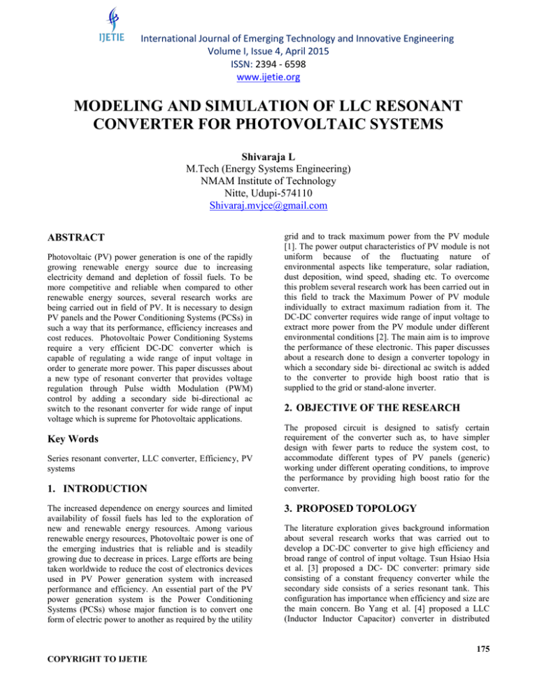
International Journal of Emerging Technology and Innovative Engineering Volume I, Issue 4, April 2015 ISSN: 2394 - 6598 www.ijetie.org MODELING AND SIMULATION OF LLC RESONANT CONVERTER FOR PHOTOVOLTAIC SYSTEMS Shivaraja L M.Tech (Energy Systems Engineering) NMAM Institute of Technology Nitte, Udupi-574110 Shivaraj.mvjce@gmail.com ABSTRACT Photovoltaic (PV) power generation is one of the rapidly growing renewable energy source due to increasing electricity demand and depletion of fossil fuels. To be more competitive and reliable when compared to other renewable energy sources, several research works are being carried out in field of PV. It is necessary to design PV panels and the Power Conditioning Systems (PCSs) in such a way that its performance, efficiency increases and cost reduces. Photovoltaic Power Conditioning Systems require a very efficient DC-DC converter which is capable of regulating a wide range of input voltage in order to generate more power. This paper discusses about a new type of resonant converter that provides voltage regulation through Pulse width Modulation (PWM) control by adding a secondary side bi-directional ac switch to the resonant converter for wide range of input voltage which is supreme for Photovoltaic applications. Key Words Series resonant converter, LLC converter, Efficiency, PV systems 1. INTRODUCTION The increased dependence on energy sources and limited availability of fossil fuels has led to the exploration of new and renewable energy resources. Among various renewable energy resources, Photovoltaic power is one of the emerging industries that is reliable and is steadily growing due to decrease in prices. Large efforts are being taken worldwide to reduce the cost of electronics devices used in PV Power generation system with increased performance and efficiency. An essential part of the PV power generation system is the Power Conditioning Systems (PCSs) whose major function is to convert one form of electric power to another as required by the utility grid and to track maximum power from the PV module [1]. The power output characteristics of PV module is not uniform because of the fluctuating nature of environmental aspects like temperature, solar radiation, dust deposition, wind speed, shading etc. To overcome this problem several research work has been carried out in this field to track the Maximum Power of PV module individually to extract maximum radiation from it. The DC-DC converter requires wide range of input voltage to extract more power from the PV module under different environmental conditions [2]. The main aim is to improve the performance of these electronic. This paper discusses about a research done to design a converter topology in which a secondary side bi- directional ac switch is added to the converter to provide high boost ratio that is supplied to the grid or stand-alone inverter. 2. OBJECTIVE OF THE RESEARCH The proposed circuit is designed to satisfy certain requirement of the converter such as, to have simpler design with fewer parts to reduce the system cost, to accommodate different types of PV panels (generic) working under different operating conditions, to improve the performance by providing high boost ratio for the converter. 3. PROPOSED TOPOLOGY The literature exploration gives background information about several research works that was carried out to develop a DC-DC converter to give high efficiency and broad range of control of input voltage. Tsun Hsiao Hsia et al. [3] proposed a DC- DC converter: primary side consisting of a constant frequency converter while the secondary side consists of a series resonant tank. This configuration has importance when efficiency and size are the main concern. Bo Yang et al. [4] proposed a LLC (Inductor Inductor Capacitor) converter in distributed 175 COPYRIGHT TO IJETIE International Journal of Emerging Technology and Innovative Engineering Volume I, Issue 4, April 2015 ISSN: 2394 - 6598 www.ijetie.org power systems. This topology has advantages such as reduced switching losses, conduction losses which resulted in increase in efficiency by 2-3%. Similar research works were carried out on LLC converter by Reza Beiranvand et al. [5] [6], Yue chen et al. [7], Fariborz Musavi et al. [8] to improve the performance while reducing the cost of electronics. Taking the literature as guidance, a new topology as shown in Figure1 is developed to design a high efficiency LLC resonant converter and inverter for Photovoltaic systems. The proposed LLC converter is based on the principle of series resonant converter. The series resonant converter is efficient because it allows direct power transfer to the load and the primary side MOSFET attains Zero Voltage Switching (ZVS) while secondary side Diode attains Zero Current Switching (ZCS). But the drawback in Series resonant converter is insufficient input voltage regulation needed for PV systems. The proposed topology is a hybrid series resonant with PWM boost converter which makes use of high frequency bi directional AC MOSFET and achieves wide range of input with fixed frequency control. The operating principle of the LLC converter is similar to the resonant converter along with a clip circuit to double the voltage. The primary side of isolation transformer is a full bridge switching network consisting of switches S1 to S4 to lower the switch count and also the network operates at series resonant frequency, fr (expressed in equation 1). The secondary side of isolation transformer consists of a bidirectional switch (MOSFET), S5. To determine resonant frequency fr, the secondary side resonant inductor Lr and resonant capacitor Cr1, Cr2. Certain assumptions are made for simplification of the proposed converter topology. They are: i. ii. iii. Co is greater than VO, Cr1, and Cr2. Cr1, Cr2 are equal. Lm is greater than Lr. f …. (1) Figure1: Proposed LLC resonant converter The bidirectional ac switch is devised as a two drain connected MOSFET. When S5 is turned on, fr is doubled, secondary transformer is shorted and Lr steps in as boost inductor. When S5 is turned off, Lr oscillates Cr1, Cr2. Once this process is completed the inverter operation is triggered. 3.1 Modes Of Operation To completely understand the proposed topology, the circuit can be explained in three modes: PWM boost mode, series resonant mode and idle mode. MODE 1-[t0< t < t1] PWM boost mode: In this mode, S1 and S4 conduct to produce a positive voltage in the primary side of the transformer. The secondary winding of the transformer gets shorted when switch S5 conducts due to which current in the leakage inductance is nearly zero and the voltage across Cr1 is lower. The average voltage of the resonant capacitance, Vcr1 is half of the output voltage . The voltage ripple of the resonant capacitance is given by, (expressed in equation 2). The voltage across the resonant capacitor during all the operating mode is given by, vcr2 = V0 – vcr1. ……………….. (2) ……………… (3) In this mode, when S5 is turned on leakage inductor steps in as boost inductor and the current in it increases linearly (expressed in equation 3). Similarly when switch S2 and S3 conduct in the second cycle, a negative voltage is 176 COPYRIGHT TO IJETIE International Journal of Emerging Technology and Innovative Engineering Volume I, Issue 4, April 2015 ISSN: 2394 - 6598 www.ijetie.org produced on the primary side of the transformer and the converter steps in the second PWM mode. MODE 3-[t2< t < t3] idle mode: In this mode, the current in Lr decreases to zero (expressed in equation 5) and the converter operates in idle mode. During this mode there is no power transfer from source to load. At this condition, the circuit operates at a constant frequency. ZCS is achieved on the secondary side of the output diode, ZVS is achieved on the primary side of the MOSFET and the switches S1 and S4 turn off. During this period the voltage across Cr1 is higher (expressed in equation 6). ……… (5) ……………. (6) Figure2: PWM boost mode operation MODE 2-[t1 < t < t2] series resonant mode: In this mode switch S5 turns off and the converter operates as a series resonant converter. The resonant inductor Lr that was charged in mode 1 (expressed in equation 4), discharges in mode 2 through the parallel combination of Cr1 and Cr2. The operating voltage required by the inverter is obtained in this mode and it is triggered. Similarly after S2 and S3 turns on in second part, the ac switch S5 turns off again to step into series resonant mode again and the process repeats. …………. (4) Figure4: Idle mode operation 3.2 Design Procedure Of Converter The transformer turns ratio „n‟ (expressed in equation 7) should be selected in such a way that the nominal input voltage should produce appropriate output voltage. …………… (7) Cr (expressed in equation 8) is selected depending on the required resonant frequency. It should be larger than Lr as it affects the voltage rating of switch S5 to reduce the voltage across S5 and Cr. The value of Lr (expressed in equation 9) is chosen in such that the ratio between leakage inductance and magnetizing inductance will produce appropriate conversion ratio within the range of required frequency. The design procedure of this topology has higher Lm/ Lr ratio. Figure3: Series resonant mode operation …………..… (8) 177 COPYRIGHT TO IJETIE International Journal of Emerging Technology and Innovative Engineering Volume I, Issue 4, April 2015 ISSN: 2394 - 6598 www.ijetie.org ………… (9) 4. SIMULATION AND RESULTS A LLC converter consisting of DC input source, full bridge inverter, full bridge LLC resonant converter, high frequency transformer, half bridge rectifier, filter circuit and resistive load is shown in the figure 5. The DC input voltage is inverted to AC by the full bridge MOSFET which in turn is connected to primary side of the transformer. The secondary side of the transformer is connected to the LLC resonant tank circuit. The output voltage of the resonant tank circuit is converted to DC by the half bridge rectifier, which is then doubled by the clip circuit and fed to the inverter. The full bridge inverter converts the DC voltage to AC and synchronizes the switching frequency and output frequency, which is then, supplied to the AC grid or standalone systems. Do1,Do2 n Lm Lr Cr1,Cr2 C0 Cin IN4007 5 713.3μH 33.5μH 100nF 1.2μF 88μF Figure6. Output voltage of S1, S2, S3, S4 and S5. Figure5. LLC converter with inverter The simulation of LLC converter is done using MATLAB and the results obtained are shown below. The waveforms of DC input voltage, MOSFET output voltage of S1, S2 and S4 are shown in Figure6. The simulated output (voltage and current) of the proposed converter is shown in Figure8. The steady state output voltage and current of inverter is shown in Figure7 and 9 respectively. The specification parameters of elements used in the simulation circuit is shown in the Table 1. Figure7. Steady state output current of inverter. Table 1: Parameters used in the simulation Elements fs S1-S4 S5 Values/Specification 130kHz IRFZ48 IRF640 178 COPYRIGHT TO IJETIE International Journal of Emerging Technology and Innovative Engineering Volume I, Issue 4, April 2015 ISSN: 2394 - 6598 www.ijetie.org 6. ACKNOWLEDGEMENT I have a great pleasure in expressing my deep sense of gratitude to the Management of Nitte and my guide Prof. Rajaneesh Acharya for supporting and encouraging me throughout the project. I would like to thank my parents and friends who have stood as a pillar of support throughout the entire journey. 7. REFERENCES Figure8. Simulation output of proposed converter. Figure9. Steady state output voltage of inverter. 5. CONCLUSION The increase in energy demand and growth in PV has made it is necessary to improve the performance and reduce the cost of electronic devices used in Power Conditioning systems. Generally, the converter in PCS has certain design requirements like wide range of input voltage, high efficiency, high boost ratio, high output power etc. that is difficult to obtain. So taking this as a main concern, the proposed LLC converter along with the inverter achieved these requirements by ZCS of output diodes, ZVS of switches of primary side, direct power transfer to the load and low circulating current. The simulation of the proposed converter with inverter topology resulted with an output voltage nearer 320V which is ideal for PV systems. 1) PCSs for Renewables, Storage, Microgrid, “www.nist.gov/el/smartgrid/powercon.cfm” ,Jan 24,2014 2) Thomas Labella, Wensong Yu, Jih- sheng Lai, Matthew Senesky, David Anderson, “ A Bidirectional- switch based wide input range High efficiency isolated Resonant converter for Photovoltaic applications”, IEEE transactions on power electronics , Vol. 29, No.7, July 2014. 3) T.-H. Hsia, H.-Y. Tsai, D.chen, M. Lee, and C.-S. Huang, “Interleaved active-clamping converter with ZVS/ZCS features,” IEEE Trans. Power Electron., vol.26 no.1, pp.29-37, Jan.2011. 4) B. Yang, F. C. Lee, A. J. Zhang, and G. Huang, “LLC resonant converter for front end DC/DC conversion”, APEC 2002, vol.2, pp. 1108-1112. 5) R. Beirand, B. Rashidian, M. R. Zolghadri and S. M. H. Alavi, “A design procedure for optimizing the LLC resonant converter as a wide output range voltage source”, IEEE conference on power electronics, vol 27, no.8, pp 3749-3763, 2012. 6) R. Beirand, B. Rashidian, M. R. Zolghadri and S. M. H. Alavi” using LLC resonant converter for designing wide range voltage source”, IEEE transactions, vol.58, n0.5, pp-1746-1756, May 2011. 7) Y. Chen, X. Wu, Z. Qianand W. Zhang, “Design and optimization of a wide output voltage range LED driver based on LLC resonant topology”, ICPE & ECCE-2011, pp.2831-2837. 8) F. Musavi, M. Craciun, D. S. Gautam, W. Eberle and W.G. Dunford, “An LLC resonant DC-Dc converter for wide output voltage range battery charging application”, IEEE transaction on power electronics, vol no.99, p 1-1, Dec 2013. 179 COPYRIGHT TO IJETIE

