Development of FPGA Based Data Acquisition System
advertisement

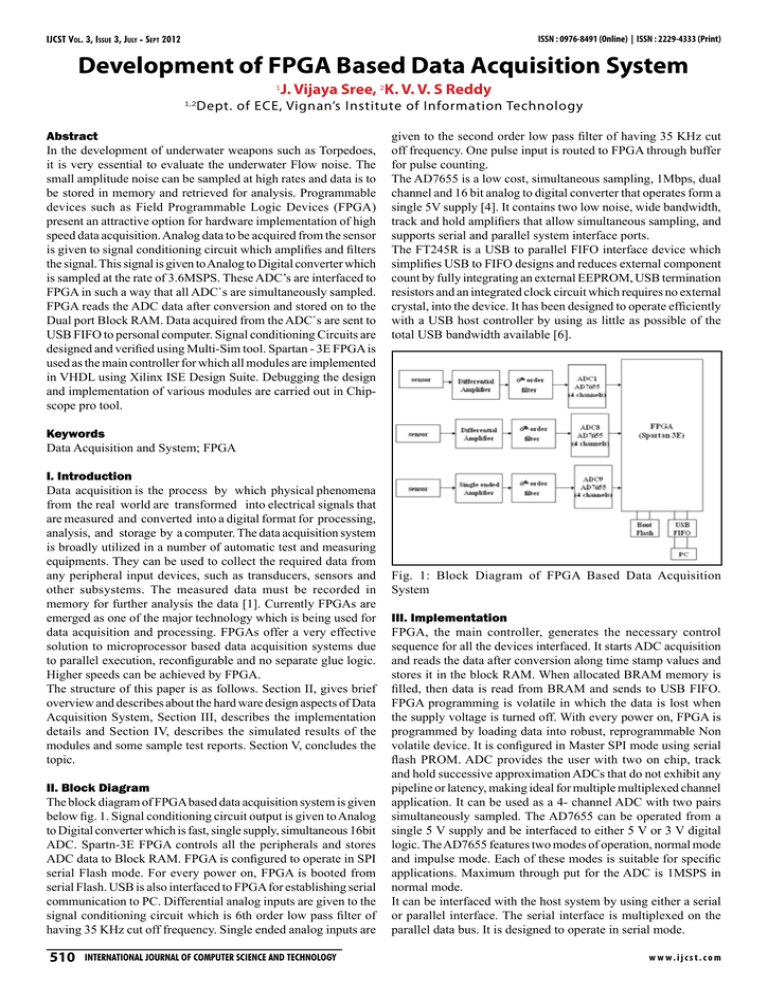
ISSN : 0976-8491 (Online) | ISSN : 2229-4333 (Print) IJCST Vol. 3, Issue 3, July - Sept 2012 Development of FPGA Based Data Acquisition System 1 1,2 J. Vijaya Sree, 2K. V. V. S Reddy Dept. of ECE, Vignan’s Institute of Information Technology Abstract In the development of underwater weapons such as Torpedoes, it is very essential to evaluate the underwater Flow noise. The small amplitude noise can be sampled at high rates and data is to be stored in memory and retrieved for analysis. Programmable devices such as Field Programmable Logic Devices (FPGA) present an attractive option for hardware implementation of high speed data acquisition. Analog data to be acquired from the sensor is given to signal conditioning circuit which amplifies and filters the signal. This signal is given to Analog to Digital converter which is sampled at the rate of 3.6MSPS. These ADC’s are interfaced to FPGA in such a way that all ADC`s are simultaneously sampled. FPGA reads the ADC data after conversion and stored on to the Dual port Block RAM. Data acquired from the ADC`s are sent to USB FIFO to personal computer. Signal conditioning Circuits are designed and verified using Multi-Sim tool. Spartan - 3E FPGA is used as the main controller for which all modules are implemented in VHDL using Xilinx ISE Design Suite. Debugging the design and implementation of various modules are carried out in Chipscope pro tool. given to the second order low pass filter of having 35 KHz cut off frequency. One pulse input is routed to FPGA through buffer for pulse counting. The AD7655 is a low cost, simultaneous sampling, 1Mbps, dual channel and 16 bit analog to digital converter that operates form a single 5V supply [4]. It contains two low noise, wide bandwidth, track and hold amplifiers that allow simultaneous sampling, and supports serial and parallel system interface ports. The FT245R is a USB to parallel FIFO interface device which simplifies USB to FIFO designs and reduces external component count by fully integrating an external EEPROM, USB termination resistors and an integrated clock circuit which requires no external crystal, into the device. It has been designed to operate efficiently with a USB host controller by using as little as possible of the total USB bandwidth available [6]. Keywords Data Acquisition and System; FPGA I. Introduction Data acquisition is the process by which physical phenomena from the real world are transformed into electrical signals that are measured and converted into a digital format for processing, analysis, and storage by a computer. The data acquisition system is broadly utilized in a number of automatic test and measuring equipments. They can be used to collect the required data from any peripheral input devices, such as transducers, sensors and other subsystems. The measured data must be recorded in memory for further analysis the data [1]. Currently FPGAs are emerged as one of the major technology which is being used for data acquisition and processing. FPGAs offer a very effective solution to microprocessor based data acquisition systems due to parallel execution, reconfigurable and no separate glue logic. Higher speeds can be achieved by FPGA. The structure of this paper is as follows. Section II, gives brief overview and describes about the hard ware design aspects of Data Acquisition System, Section III, describes the implementation details and Section IV, describes the simulated results of the modules and some sample test reports. Section V, concludes the topic. II. Block Diagram The block diagram of FPGA based data acquisition system is given below fig. 1. Signal conditioning circuit output is given to Analog to Digital converter which is fast, single supply, simultaneous 16bit ADC. Spartn-3E FPGA controls all the peripherals and stores ADC data to Block RAM. FPGA is configured to operate in SPI serial Flash mode. For every power on, FPGA is booted from serial Flash. USB is also interfaced to FPGA for establishing serial communication to PC. Differential analog inputs are given to the signal conditioning circuit which is 6th order low pass filter of having 35 KHz cut off frequency. Single ended analog inputs are 510 International Journal of Computer Science And Technology Fig. 1: Block Diagram of FPGA Based Data Acquisition System III. Implementation FPGA, the main controller, generates the necessary control sequence for all the devices interfaced. It starts ADC acquisition and reads the data after conversion along time stamp values and stores it in the block RAM. When allocated BRAM memory is filled, then data is read from BRAM and sends to USB FIFO. FPGA programming is volatile in which the data is lost when the supply voltage is turned off. With every power on, FPGA is programmed by loading data into robust, reprogrammable Non volatile device. It is configured in Master SPI mode using serial flash PROM. ADC provides the user with two on chip, track and hold successive approximation ADCs that do not exhibit any pipeline or latency, making ideal for multiple multiplexed channel application. It can be used as a 4- channel ADC with two pairs simultaneously sampled. The AD7655 can be operated from a single 5 V supply and be interfaced to either 5 V or 3 V digital logic. The AD7655 features two modes of operation, normal mode and impulse mode. Each of these modes is suitable for specific applications. Maximum through put for the ADC is 1MSPS in normal mode. It can be interfaced with the host system by using either a serial or parallel interface. The serial interface is multiplexed on the parallel data bus. It is designed to operate in serial mode. w w w. i j c s t. c o m IJCST Vol. 3, Issue 3, July - Sept 2012 ISSN : 0976-8491 (Online) | ISSN : 2229-4333 (Print) The chip-scope simulation results show the initiation of ADC for every 5µsec and conversion is completed by 1µsec and data is available for reading in SPI mode by 64 Serial clock cycles. Fig. 2: FPGA Control Flow The AD7655 is configured to use in the slave serial interface when the SER/PAR is held high. The AD7655 outputs 32 bits of data, MSB first, on the SDOUT pin. The order of the channels being output is also controlled by A/B. When high, Channel A is output first; when low, Channel B is output first. This data is synchronized with the 32 clock pulses provided on the SCLK pin. Fig. 3: ADC Control Sequence The control flow of the ADC which is implemented in VHDL [2] is shown in fig. 3. Each ADC chip has got four channels and conversion start signal is required for ADC to start conversion. ADC sampling required for all channel is to be at 100 KHz. For every conversion start, ADC gives out two channels of data serially. So conversion start frequency will be 200 KHz to read out four channel data. For every 5µs, conversion signal must be initiated. When it goes to T1, conversion is initiated and goes to T3, after conversion is over. Two channel data is read from SDOUT pin from MSB to LSB by 32 clock pulses. When the ADC data available signal is High, then ADC data is written to the Block RAM. V. Simulation Results In the signal conditioning circuits, multiple feedback filters are designed to have high Q value and high gain. These circuits are designed and simulated and verified in NI Multisim 11.1 software. These are the simulated results for the 2nd order low pass filters. Table 1: Simulated results for LPF For a Single ended Channel For a differential channel Input voltage (Vin in Vp-p) Frequency in KHz o/p voltage Range in Vp-p I/p voltage (Vin in Vp-p) 10V 10 4.72-4.80 200mV 10 4.56-4.72 33 3.92-4.08 33 3.52-3.60 35 3.84-4.0 35 3.36-3.52 38 3.68-3.84 38 3.20-3.28 40 3.52-3.68 40 3.04-3.12 w w w. i j c s t. c o m Frequency in KHz o/p voltage Range in Vp-p Fig. 4: ADC Conversion Debugging by Chip-Scope Pro The following results are the chip-scope outputs for data to be written onto the USB. Fig. 5: Chip-Scope Results for Data Writing to USB VI. Conclusion The Data Acquisition System has advantages of small size, light weight and low-power consumption. It can be used in a variety of situations. The system uses AD7655 with high speed . The USB2.0 interface ensured the data accurate and fast upload, it meets fully the real-time requirement. References [1] John Park, Steve Mackay,"Practical Data Acquisition for instrumentation & control system". [2] FT245R USB FIFO IC Datasheet. [3] Pong P. Chu,"FPGA Prototyping by VHDL Examples Xilinx SpartanTM-3 version". [4] The Design Warrior’s Guide to FPGAs--Clive “Max” Maxfield ". [5] Jayaram Bhasker,"A VHDL Primer". [6] Volnei A.Pedroni,"Circuit Design with VHDL". [7] Hernandez, Rodriguez, Giron, Mateos, Cobreces,“A DSP- and FPGA based Industrial control with High-speed communication interfaces for grid converters applied to distributed power generation systems”, IEEE Transactions, 2009, pp- 654 – 669. International Journal of Computer Science And Technology 511


