Data Sheet
AD1520
Du a l Ch a n n e l 1 . 5 GS PS
A n a l o g I n p u t X M C/ PM C
Applications
w
Electronic Warfare (EW)
w
Electronic Counter Measures (ECM)
w
Spectral Analysis
w
RADAR
Features
w
2 Channel 1.5GSPS, 8-bit ADC
w
Xilinx® Virtex®-5 SX95T FPGA (user programmable)
w
Dual banks of QDR2 SRAM and DDR2 SDRAM memories
w
Capable of multi-board synchronization
w
XMC/PMC form factor
w
Air- or conduction-cooled rugged versions
w
Windows®, VxWorks® and Linux® support
Benefits
w
Combined acquisition and data processing
w
Lower power solution
w
Industry standard form factor
w
PCI Express® provides high throughput to baseboard
Overview
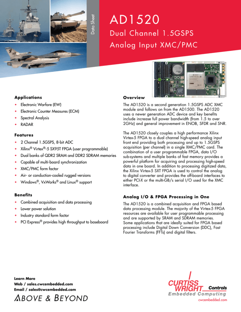
The AD1520 is a second generation 1.5GSPS ADC XMC
module and follows on from the AD1500. The AD1520
uses a newer generation ADC device and key benefits
include increase full power bandwidth (from 1.5 to over
2GHz) and general improvement in ENOB, SFDR and SNR.
The AD1520 closely couples a high performance Xilinx
Virtex-5 FPGA to a dual channel high-speed analog input
front end providing both processing and up to 1.5GSPS
acquisition (per channel) in a single XMC/PMC card. The
combination of a user programmable FPGA, data I/O
sub-systems and multiple banks of fast memory provides a
powerful platform for acquiring and processing high-speed
data in one board. In addition to processing digitized data,
the Xilinx Virtex-5 SXT FPGA is used to control the analog
to digital converter and provides the off-board interfaces to
either PCI-X or the multi-GB/s serial I/O used for the XMC
interface.
Analog I/O & FPGA Processing in One
The AD1520 is a combined acquisition and FPGA based
data processing module. The majority of the Virtex-5 FPGA
resources are available for user programmable processing
and are supported by SRAM and SDRAM memories.
Some applications that are ideally suited for FPGA based
processing include Digital Down Conversion (DDC), Fast
Fourier Transforms (FFTs) and digital filters.
Learn More
Web / sales.cwcembedded.com
Email / sales@cwcembedded.com
cwcembedded.com
1.5GSPS Analog Input
Xilinx Virtex-5 FPGA
Analog to digital conversion is performed by a National
Semiconductor ADC08D1520 analog to digital converter,
which is a dual channel 8-bit, 1.5GSPS device. The analog
input stages are transformer AC coupled to the ADC via
a balun. Using the ADC’s built-in demultiplexer, digitized
data is transferred to the FPGA using an interleaved 32-bit
interface (2+2 samples in parallel).
The AD1520 is fitted with a Xilinx Virtex-5 SX95T FPGA
(contact Curtiss-Wright for availability of other FPGA
variants) which is optimized for a high ratio of DSP blocks
to standard logic blocks to support high performance signal
processing.
The FPGA is configured at power up from FLASH with a
default image, a recovery image or an image the customer
generates. In addition to FLASH configuration, new images
can be downloaded from the host via the PCI or PCI
Express (PCIe) interface. Software is provided to load new
images into either FLASH or SRAM. Bit streams stored in
SRAM benefit from faster downloads while bypassing nonvolatile storage - useful for secure applications.
Clocks, Triggers & Multi-board Sync
The AD1520 provides a front-panel MMCX connector for
connecting an external sample clock source (required).
A front panel mounted trigger input (TI) and a trigger
output (TO) signal are connected to the FPGA via LVPECL
I/O stages. This allows the FPGA to define the trigger
mechanism in the application for maximum flexibility.
Multiple SDRAM & SRAM Banks
The AD1520 features both external SRAM and SDRAM
connected to the FPGA. These can be used for buffering
ADC data or for general purpose processing support.
The AD1520 supports multi-board synchronization allowing
all ADCs to be synchronized to a common clock source.
When synchronized, all data will be aligned and coherent
across multiple AD1520 boards. Curtiss-Wright’s XCLK1
clock generator is capable of providing this synchronized
sample clock output to two or more AD1520 ADCs,
providing support for features such as synchronous reset of
the sample clock.
The two 128MB DDR2 SDRAM banks on the AD1520 can
be used in parallel to buffer digitized data. Each bank is
16-bits wide.
QDR2 SRAM provides higher bandwidth external memory.
Two 2M x 36-bit banks are fitted on the AD1520.
Figure 1: Multiple AD1520s can be synchronized
Analog Inputs
Trigger Input
Synchronized
Sample Clock
Sync/Sample Alignment
XCLK1
AD1520
AD1520
AD1520
2
Curtiss-Wright Controls Embedded Computing / cwcembedded.com
PCI/PCI-X, PCIe & Multi-GB/s I/O
FusionXF Software/HDL Support
The AD1520 includes a PCI/PCI-X interface, supporting
up to 133MHz operation, and a PCIe interface. These
interfaces provide multi-channel DMA support.
Curtiss-Wright’s FusionXF development kit includes software,
HDL and utilities with examples and infrastructure for using
the AD1520 or the AD3000 on one of Curtiss-Wright’s
other Xilinx Virtex-5 and Virtex-4 FPGA-based products.
FusionXF includes a C-API and sophisticated DMA support.
The PCIe interface uses the Virtex-5 FPGA’s RocketIO™ GTP
transceivers and an embedded end-point controller, which
is a hard IP block within the Virtex-5 FPGA. This built-in
PCIe endpoint block supports x4 or x8 lane communications
at 2.5GB/s according to the PCIe standard, but can be
bypassed to support other protocols like sFPDP or Serial
RapidIO® (SRIO). Overall, the Virtex-5 FPGA provides
sixteen, full duplex high-speed serial communication links
through RocketIO GTP transceivers. These links are evenly
split between two XMC (VITA 42) connectors, with each link
capable of operation at up to 3.2GB/s and can be driven
as independent data streams or bonded to create ‘fat pipes’
for fewer, but higher bandwidth, data streams.
One of the core elements to the FusionXF development
kit is a framework for adding in new IP functionality or
capabilities to the FPGA. With support for high-speed DMA
capabilities and documented interfaces for the integration
of custom IP, FusionXF makes HDL development easier and
integration more straightforward.
Example software/HDL illustrates how to interface to
on-board devices such as QDR SRAM and DDR SDRAM.
Under software running on the host, data can be moved
to and from the AD1520’s memories using FusionXF’s high
performance DMA capabilities.
Rugged Build Options
Software utilities are provided for configuring the FPGA.
These include FLASH programming and commands to
configure the FPGA from a given image in FLASH or SRAM.
The FPGA may also be configured via a ChipScope™ Pro/
JTAG interface. Host operating systems supported by the
FusionXF suite includes Windows, VxWorks and Linux.
Although the AD1520 is aimed at applications requiring
both high-speed digitization and user programmable
FPGA processing, a full acquisition-only example image is
provided. This allows the AD1520 to be used ‘out-of-thebox’ without having to develop FPGA code. This image
can be loaded from the FLASH file system and supports full
bandwidth data acquisition, external trigger modes and
high-speed DMA driven PCI-X/PCIe channels to the host
processor. This example can be modified to include a user
application, making the AD1520 quick and easy to use.
A range of environmental requirements are addressed
by the AD1520: air-cooled benign, air-cooled extended
temperature, air-cooled rugged and conduction-cooled. For
conduction-cooled applications, the host board must be able
to incorporate front panel I/O connections. Depending on
the application, a suitable heatsink may be required for
conduction-cooled builds.
3
Curtiss-Wright Controls Embedded Computing / cwcembedded.com
Analog Performance
Figure 4: AD1520 Signal to Noise Ratio
Figure 2: AD1520 Effective Number of Bits
AD1520 ENOB
50
8
48
46
7
44
42
6
SNR (dB)
ENOB (bits)
Channel A
Channel B
AD1520 SNR
Channel A
Channel B
40
38
5
36
34
4
0
500
1000
1500
2000
2500
32
Frequency (MHz)
30
0
500
1000
Frequency (MHz)
1500
2000
2500
Effective Number of Bits (ENOB)
Signal to Noise Ratio (SNR)
The AD1520 shows an ENOB greater than 7-bits for the
majority of the 1st and 2nd Nyquist zones. This drops below
8MHz and above ~1700MHz. The balun (necessary for
wide input bandwidth) at the front end is the primary cause
of the low frequency distortion; the high frequency distortion
is due in part to the ADC bandwidth and reduced SNR. The
AD1520 performance correlates favorably, within 0.2-bits,
to the National Semiconductor datasheet for frequencies up
to 1500MHz.
The AD1520 board exhibits similar characteristics to the
ADC08D1520 analog to digital converter, comparing
favorably with the National Semiconductor datasheet. The
peak SNR is at 1500MHz (vs. approximately 1250MHz
in the ADC datasheet) showing an extended performance
region of around 200MHz higher than the ADC datasheet
Figure 5: AD1520 Full Scale Power Bandwidth
Figure 3: AD1520 Spurious Free Dynamic Range
7.5
Full Scale Power (dBm)
Channel A
Channel B
AD1520 SFDR
65
60
55
50
SFDR (dB)
Channel A
Channel B
AD1520 Full Scale Power Bandwidth
9.0
45
6.0
4.5
3.0
1.5
40
0.0
35
0
500
30
1000
1500
2000
2500
Frequency (MHz)
25
20
0
500
1000
1500
2000
2500
Frequency (MHz)
Gain Bandwidth
The output is normalized to show the input signal level
required to give a full scale sampled signal. The AD1520 is
shown operating in “Extended Control” mode with the 'Full
Scale Voltage Adjust' Register set to 700mVp-p (0.88 dBm).
The output shows a 3dB bandwidth approaching 2250MHz
(i.e. almost all of 1st, 2nd and 3rd Nyquist regions) with
approximately +/- 1dB Gain Flatness in 1st and 2nd Nyquist
(0-1500MHz).
Spurious Free Dynamic Range (SFDR)
The SFDR is generally dominated by the 2nd or 3rd
harmonics of the input signal which are typically introduced
by non-linearities in the system. The main non-linear element
of the AD1520 is the balun which performs the broadband
single-ended to differential signal conversion required
for input to the ADC chip. The highest spurious signal is
sometimes located at (FSamp/2) ± FInput, this spurious signal is
caused by the internal folding interpolating architecture of
the ADC08D1520 device.
4
Curtiss-Wright Controls Embedded Computing / cwcembedded.com
Sample FFT Plots
Notes
Figure 6: Channel A Signal Frequency: 1310.9MHz (aliased
back to ~189MHz), Sample Frequency 1.5GSPS
To gather the results presented here, a spectrally pure sine
wave was applied to each input in turn and 8K of data
was collected. An 8K FFT was performed and the dynamic
parameters were calculated from the FFT. The input signal
frequencies were chosen so as to ensure coherent sampling,
which removes the need to apply a window function. This
allows greater visibility of detail in the FFT, as window
functions often hide spurious signals.
For more information on the analog characterization
of this product, please contact your local CurtissWright representative for a more complete AD1520
characterization report.
Figure 7: Channel B Signal Frequency: 1310.9MHz (aliased
back to ~189MHz), Sample Frequency 1.5GSPS
5
Curtiss-Wright Controls Embedded Computing / cwcembedded.com
Figure 8: AD1520 Block Diagram
Trigger
Output
9MB
LVPECL
QDR II SRAM
GP I/O
9MB
QDR II SRAM
36-bit
36-bit
8x RocketIO
ADC
8x RocketIO
ADC08D1520
Channel 1
Balun
ADC
Channel 2
Balun
ADC
I
Q
Xilinx
Virtex-5 FPGA
SX95T
Sample
Clock
User I/O
64-bit,
133MHz PCI-X
PCI-X/PCI-X
Bridge
16-bit
Trigger
Input
LVPECL
128MB
DDR SDRAM
128MB
DDR SDRAM
1Gbit
FLASH
Table 1: Specifications
Clock & Trigger Inputs
FPGA
Device
Xilinx Virtex-5 SX95T (speed grade 2)
External
Front panel MMCX
DDR2 SDRAM
2 banks of 64M x 16-bit (2 banks of 128MB)
Input Level
600-1800mV (sine or squarewave)
QDR2 SRAM
2 banks of 2M x 36-bit (2 banks of 9MB)
1Gbit (FPGA boot/configuration including
rescue image)
200 to 1500MSPS
FLASH
Sample Frequency
Range
Input Impedance
50 Ohm, AC coupled
Trigger Input/Output
Single-ended, 50 Ohm, LVPECL, DC coupled
Analog Input
Number of Channels
2, single-ended
XMC
Sampling Frequency
Up to 1.5GSPS
XMC P15
8x RocketIO @ 3.125GB/s or 8x PCIe
Full Scale Input Voltage
600-800 mV (programmable)
XMC P16
8x RocketIO @ 3.125GB/s
Device
ADC08D1520
Software/HDL Code
Full Power
Bandwidth (3dB)
2.2GHz
Host Drivers
Windows, VxWorks 6.x, Linux
Input Impedance
50 Ohm, AC coupled
Utilities
FLASH programming, diagnostics
SNR
46.98 dB1
Software/HDL Code
Analog input, memory interfaces, PCI-X, PCIe
SFDR
61.6 dBc1
ENOB
7.45 bits1
Weight
32/64-bit PCI 33/66MHz,
PCI-X 66/100/133MHz,
Master/slave/DMA, Interrupt support
Notes
1.Fin = 748 MHz; Vin = Full Scale - 0.5 dB; Fs = 1500 MSPS
All the analog characterizations in this datasheet represent the
measured performance of a standard production board in normal
laboratory conditions. These are typical performance figures and are not
guaranteed.
Miscellaneous
PCI
PCI Compliance
6
Commercial air-cooled 113g
Rugged air-cooled 150g
Conduction-cooled 141g
Curtiss-Wright Controls Embedded Computing / cwcembedded.com
Table 2:
Environmental Specifications
Rugged
Commercial
Air-cooled
Level
Conduction-cooled
1001
Level 1001
0°C to +55°C
(15 CFM air flow)2
-40°C to +70°C
(20 CFM air flow)2
-40°C to +70°C
(Card Edge Temp)3
Non-Operational
-40°C to +85°C
-50°C to +100°C
-50°C to +100°C
Vibration
Operational (Random)
-
0.04g2/Hz
0.1g2/Hz
Shock
Operational
-
30g peak,
11ms half sine
40g peak,
11ms half sine
Humidity
Operational
5-95%
non-condensing
Up to 95%
Up to 95%
Operational
-
-1,500 to 60,000ft
-1,500 to 60,000ft
No
Yes
Yes
Temperature
Altitude4
Conformal
Operational (at sea level)
Coating5
Notes
1.Availability of the ruggedization levels are subject to qualifications for each product.
2.For operation at altitudes above sea level, the minimum volume flow rate should be adjusted to provide the same mass flow rate as would be provided at
sea level. Additional airflow might be required if the card is mounted together with, or next to, cards that dissipate excessive amounts of heat. Some higherpowered products may require additional airflow.
3.The contacting surface on the rack/enclosure must be at a lower temperature to account for the thermal resistance between the plug-in unit and rack/
enclosure.
4.Depending on the technology used, the risk for Single Event Upsets will increase with altitude.
5.Coated with Humiseal 1B31 or 1B73EPA. (ref. http://humiseal.com for details)
*While the AD1520 is designed to meet these environmental requirements, formal qualification testing has not been performed to these levels. Please contact
your local sales representative to discuss your program specific requirements.
Warranty
The information in this document is subject to change
without notice and should not be construed as a commitment
by Curtiss-Wright Controls Embedded Computing. While
reasonable precautions have been taken, Curtiss-Wright
Controls assumes no responsibility for any errors that may
appear in this document. All products shown or mentioned
are trademarks or registered trademarks of their respective
owners.
This product has a one year warranty.
Contact Information
To find your appropriate sales representative, please visit:
Website: www.cwcembedded.com/sales
Email: sales@cwcembedded.com
For technical support, please visit:
Website: www.cwcembedded.com/support1
© Copyright 2008, Curtiss-Wright Controls, Inc.,
All Rights Reserved. MKT-DS-AD1520-06089v4
Email: support1@cwcembedded.com
7
Curtiss-Wright Controls Embedded Computing / cwcembedded.com
