Indy® R500 Reader Chip (IPJ-R500)
Electrical, Mechanical, & Thermal Specification
Indy® R500 Reader Chip Overview
Air Interface Protocol
EPCglobal UHF Class 1 Gen 2 / ISO 18000-6C
• DSB and PR-ASK transmit modulation modes
• Dense reader mode (DRM)
Integrated Power
Amplifier
Configurable up to 17 dBm. External power amplifier supported for high performance
applications
Transmit Output Power
Adjustable to > 25 dB
Modem
Configurable digital baseband
Operating Frequencies
860–960 MHz
Package
64-pin 9 mm x 9 mm x 0.85 mm QFN
Power
Low power consumption, 1100 to 800 mW configuration dependent; 200µW standby
Process
0.18 µm SiGe BiCMOS
RSSI
Per tag, configurable bandwidth
Sensitivity
-68 dBm (DRM, M4 with LF 250KHz)
Supported Regions
Configurable for world wide usage
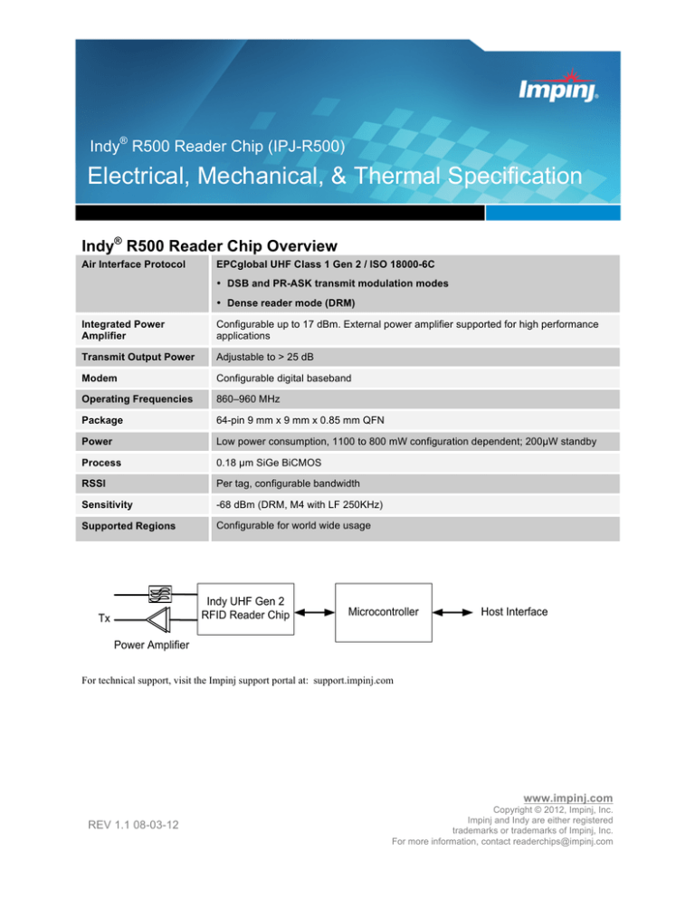
Indy UHF Gen 2
RFID Reader Chip
Tx
Microcontroller
Host Interface
Power Amplifier
For technical support, visit the Impinj support portal at: support.impinj.com
www.impinj.com
REV 1.1 08-03-12
Copyright © 2012, Impinj, Inc.
Impinj and Indy are either registered
trademarks or trademarks of Impinj, Inc.
For more information, contact readerchips@impinj.com
TABLE OF CONTENTS
1 INTRODUCTION ..................................................................................................................................................1 1.1 TERMINOLOGY ...................................................................................................................................................1 1.2 REFERENCE DOCUMENTS ...................................................................................................................................2 2 ABOUT THIS DOCUMENT ................................................................................................................................4 3 PIN LISTING/SIGNAL DEFINITIONS .............................................................................................................5 3.1 PIN LISTING AND SIGNAL DEFINITIONS ..............................................................................................................5 4 ELECTRICAL SPECIFICATIONS ....................................................................................................................7 4.1 ABSOLUTE MAXIMUM RATINGS.........................................................................................................................7 4.2 OPERATING CONDITIONS....................................................................................................................................7 4.3 TRANSCEIVER FUNCTIONAL SPECIFICATIONS ....................................................................................................8 5 FUNCTIONAL DESCRIPTION ........................................................................................................................11 5.1 ANALOG RECEIVER INTERFACES......................................................................................................................12 5.1.1 Receiver Front-end Circuitry ....................................................................................................................12 5.1.2 PLL Loop Filter ........................................................................................................................................12 5.1.3 Receive RF Interface .................................................................................................................................12 5.2 ANTENNA CONFIGURATION SCENARIOS ..........................................................................................................12 5.3 RF POWER DETECTION ....................................................................................................................................14 6 FREQUENCY GENERATION ..........................................................................................................................15 6.1 INTERNAL SYNTHESIZER...................................................................................................................................15 7 DEVICE CONTROL AND PROGRAMMING ................................................................................................17 7.1 SERIAL INTERFACE ...........................................................................................................................................18 7.1.1 Parallel Interface ......................................................................................................................................19 8 PACKAGE INFORMATION .............................................................................................................................21 8.1 PACKAGE INFORMATION ..................................................................................................................................21 FIGURES
FIGURE 1: LOCAL OSCILLATOR INPUT EXTERNAL INTERFACES ....................................................................................12
FIGURE 2: SINGLE ANTENNA SCENARIO ........................................................................................................................13
FIGURE 3: DUAL ANTENNA SCENARIO ..........................................................................................................................13
FIGURE 4: VCO TUNING CURVES ...................................................................................................................................15
FIGURE 5: SYNTHESIZER PHASE NOISE ...........................................................................................................................16
FIGURE 6: PLL SETTLING TIME ......................................................................................................................................16
FIGURE 7: SERIAL INTERFACE FRAME FORMAT .............................................................................................................18
FIGURE 8: SERIAL INTERFACE T2R TIMING ...................................................................................................................18
FIGURE 9: SERIAL INTERFACE R2T TIMING ...................................................................................................................19
FIGURE 10: PARALLEL INTERFACE READ TIMING .........................................................................................................19
FIGURE 11: PARALLEL INTERFACE WRITE TIMING ........................................................................................................20
FIGURE 12: INDY®R500 READER CHIP PACKAGE TOP VIEW .........................................................................................21
FIGURE 13: INDY®R500 READER CHIP PACKAGE DIMENSIONS .....................................................................................22
TABLES
Revision 1.1, Copyright © 2012, Impinj, Inc.
iii
TABLE 1: TERMINOLOGY .................................................................................................................................................1 TABLE 2: PROTOCOL SPECIFICATION DOCUMENTS .........................................................................................................3 TABLE 3: LOCAL REGULATION DOCUMENTS...................................................................................................................3 TABLE 4: SUPPLEMENTAL DOCUMENTS ..........................................................................................................................3 TABLE 5: PIN LISTING AND SIGNAL DEFINITIONS ............................................................................................................5 TABLE 6: ABSOLUTE MAXIMUM RATINGS ......................................................................................................................7 TABLE 7: OPERATING CONDITIONS.................................................................................................................................7 TABLE 8: POWER CONSUMPTION SPECIFICATIONS IN MISSION MODE (READING TAGS) AND RESET..............................8 TABLE 9: INDY R500 READER CHIP—RECEIVER SPECIFICATIONS ..................................................................................8 TABLE 10: INDY®R500 READER CHIP—TRANSMITTER SPECIFICATIONS .......................................................................8 TABLE 11: INDY®R500 READER CHIP ENVELOPE DETECTORS ........................................................................................9 TABLE 12: INDY®R500 READER CHIP SYNTHESIZER.......................................................................................................9 TABLE 13: INDY R500 READER CHIP CLOCK OUTPUT, DACS, AND ADCS...................................................................10 TABLE 14: INDY®R500 READER CHIP DIGITAL INTERFACE ..........................................................................................10 TABLE 15: INDY R500 MODES.......................................................................................................................................17 TABLE 16: PIN FUNCTIONALITY PER MODE ...................................................................................................................17 TABLE 17: SERIAL INTERFACE TIMING REQUIREMENTS ................................................................................................19 TABLE 18: PARALLEL INTERFACE TIMING CONDITIONS ................................................................................................20 iv
Revision 1.1, Copyright © 2012, Impinj, Inc.
1
Introduction
The Impinj® Indy®R500 UHF Gen 2 RFID reader chip is based on the industry leading Indy®R2000 silicon architecture. The
R500 is pin compatible with the R2000 reader chip and operates on the same software platform as the R1000 and R2000 reader
chips. The R500 compliments the Indy platform by enabling a cost-optimized solution for applications requiring moderate read
range of small tag populations. The Indy R500 read range can vary from a few meters to a few inches depending on the
following factors: transmit output power, reader antenna properties and tag performance.
The Indy R500 reader chip supports worldwide UHF industrial, science, and medical (ISM) band. The Indy R500 reader chip
comprises all of the RF and baseband blocks to interrogate and receive data from compatible RFID tags, specifically:
•
High compression point quadrature down-converting mixer
•
Fully integrated voltage controlled oscillator (VCO) supporting 840 to 960Mhz operation
•
Variable receiver (RX) gain control
•
Integrated Power Amplifier (PA), up to 20dBm peak power
•
Integrated RF envelope detectors for forward and reverse power sense
•
Integrated multipurpose Analog-to-Digital Converts (ADCs) and Digital-to-Analog Converters (DACs)
•
Configurable baseband DSP processing offers numerous configurations and optimal performance
When used in the Indy Development Platform, which includes an example protocol processor and radio control implementation,
the result is a fully functional UHF Gen 2 RFID reader.
1.1
Terminology
Table 1: Terminology
Term
Description
ADC
Analog-to-Digital Converter
AGC
Automatic Gain Control
AM
Amplitude Modulation
ASK
Amplitude Shift Keying
AUX
Auxiliary
BPF
Bandpass Filter
Class 0
Tags and readers conforming to MIT Auto-ID Center, Class 0 RFID Tag Protocol Specification
CORDIC
COordinate Rotation DIgital Computer
CW
Continuous Wave
DAC
Digital-to-Analog Converter
DFT
Discrete Fourier Transform
DRM
Dense Reader Mode
DSB
Double Sideband
EOT
End of Transfer
EPC
Electronic Product Council
FCC
Federal Communications Commission (US Regulatory Body)
FIFO
First In, First Out
Revision 1.1, Copyright © 2012, Impinj, Inc.
1
Term
Description
FIR
Finite Impulse Response
I
In-phase
IF
Intermediate Frequency
IIR
Infinite Impulse Response
I-Q
In-phase Quadrature
ISM
Industrial, Science, and Medical
ISO
International Standards Organization
ISO18000
Tags and Readers conforming to ISO/IEC FDIS 18000-6:2003(E)
LBT
Listen Before Talk
LFSR
Linear Feedback Shift Registers
LNA
Low Noise Amplifier
LO
Local Oscillator
LUT
Lookup Table
MSB
Most Significant Bit
MSps
Mega Samples per Second
NCO
Numerically Controlled Oscillator
PA
Power Amplifier
PER
Packet Error Rate
PLL
Phase Locked Loop
PoE
Power over Ethernet
PR
Phase Reversal
Q
Quadrature-phase
RF
Radio Frequency
RFID
Radio Frequency Identification
RSSI
Received Signal Strength Indicator
RX
Receiver
SJ
Self Jammer—also known as Tx carrier present at the Rx port
SJC
Self Jammer cancellation—circuitry that removes SJ from Rx port
SSB
Single Sideband
TBD
To Be Determined
TX
Transmitter
TCXO
Temperature Compensated Crystal Oscillator
UHF
Ultra High Frequency
VCO
Voltage Controlled Oscillator
1.2
Reference Documents
The Indy R500 reader chip is fully compliant with the protocol specifications provided in Table 2, as well as with the local
regulations referenced in Table 3.
2
Revision 1.1, Copyright © 2012, Impinj, Inc.
Table 2: Protocol Specification Documents
Document
ISO/IEC FDIS 18000-6C Jan. 2005
Table 3: Local Regulation Documents
Document
FCC 47 CFR Ch. 1, part 15 10-1-98 Edition
ETSI EN 302 208-1 V1.1.1
Table 4 lists supplemental information sources for the Indy R500 reader chip. Contact an Impinj representative to obtain the latest
document revisions.
Table 4: Supplemental Documents
Document
Indy R2000 Development Platform Operation
Indy Firmware Datasheet
Indy Host Library API Reference Manual
Indy Host Interface Packet Definitions
Indy OEM Configuration
Indy Host Library SDK Getting Started Guide
Indy MAC Command Definitions
Indy MAC Register Set Definitions
Revision 1.1, Copyright © 2012, Impinj, Inc.
3
2
About this document
This document constitutes the electrical, mechanical, and thermal specifications for the Indy R500 reader chip. It contains a
functional overview, mechanical data and targeted electrical specifications.
4
Revision 1.1, Copyright © 2012, Impinj, Inc.
3
Pin Listing/Signal Definitions
3.1
Pin Listing and Signal Definitions
The Indy R500 reader chip package offers pin compatibility with the R2000 package. The R500 is intended to be able to drop-in
to an R2000 board design for many applications.
The Indy R500 primarily differs from the Indy R2000 with pins 51-54 and 58-61 from a pin perspective; this restricts access to
the output of the front-end mixer where an external DRM filter would be used. All Indy chips including the Indy R500 have
internal DRM filtering which is sufficient for moderate RF noise environments; external DRM filtering enables higher immunity
in high RF noise environments.
Table 5: Pin Listing and Signal Definitions
Pin #
Pin Name
Type
+
Description
1
NC
No Connection
2
NC
3
Vdd_rx_rf
3.3 V
Supply for receive RF
4
5
RX_p
RF In
Differential receive RF Input
6
7
Atest0
A
Analog Test Bus
8
9
LO_p
RF In
Differential RF input from a high impedance tap on transmit
path. This port can be used to access the LO power detector
for possible use in fwd power control.
10
11
Atest2
A
Analog Test Bus
12
NC
13
NC
14
ADC0
A In
Voltage input to AUX ADC
15
Vdd_tx_RF
3.3 V
Supply for transmit RF, except for power amplifier
16
Vdd_tx_pre
1.8 V
Power amplifier pre-driver supply
17
Vdd_tx_pa
1.8 V
Power amplifier supply
18
ADC1
A In
Voltage input to AUX ADC
19
PA_p
RF Out
Transmit output for all modes
20
PA_n
21
Vdd_tx_ana
3.3 V
Supply for transmit analog
22
PA_modp
A out
23
PA_modn
Differential output voltage of PA modulator DAC to apply
amplitude modulation to the PA
24
ADC2
A In
Voltage input to AUX ADC
25
Detector_p
RF In
Differential peak detector input
26
Detector_n
27
DAC0
A out
Output of AUX DAC
RX_n
Atest1
LO-n
Atest3
Revision 1.1, Copyright © 2012, Impinj, Inc.
No Connection
5
Pin #
Type
Description
DAC1
29
TEST PIN
30
chip_resetn
D In
31
CLK_out
DO
32
Vdd_dig
1.8 V
33
Vdd_io
3.3 V
34
DA0
D Bi
Bidirectional data interface
35
DA1
36
DA2
37
DA3
38
ALE
D In
Address Latch Enable
39
CSn
D In
Active-low chip select, active low
30
RDn
D Bi
Read strobe, active low
41
WRn
D In
Write strobe, active low
42
IRQn
D Bi
Interrupt, active low
43
Dtest0
D Bi
Digital test bus
44
Dtest1
D Bi
Digital test bus
45
TCXO_e
D In
TCXO supply switch enable, active high
46
Vdd_TCXO
3.3 V
Input to TCXO supply switch
47
TCXO_supply
DO
Output from TCXO supply switch
48
Vdd_clkref
Supply of clock reference input buffer
49
TCXO
Reference clock from a 24 MHz AC coupled input
50
Vdd_pll
51
NC
52
NC
53
NC
54
NC
55
PLL_fil0
56
PLL_fil1
57
Vdd_vco
58
NC
59
NC
60
NC
61
NC
62
Vdd_rx_ana
63
NC
64
NC
GND
A out
+
28
Paddle
+
Pin Name
3.3 V
Output of AUX DAC
Supply of phase locked loop
No Connection
No Connection
A
Nodes for external PLL filter
3.3 V
No Connection
No Connection
3.3 V
Supply for receive analog
No Connection
GND
Single Chip Ground
In the Type column, A denotes analog, while D denotes digital. NC denotes “no connection”.
6
Revision 1.1, Copyright © 2012, Impinj, Inc.
4
Electrical Specifications
4.1
Absolute Maximum Ratings
The absolute maximum ratings (see Table 6) define limitations for electrical and thermal stresses. These limits prevent permanent
damage to the Indy R500 reader chip.
Caution:
Operation outside these maximum ratings might result in permanent damage to the device.
Table 6: Absolute Maximum Ratings
Parameter
Conditions
Min.
Max.
Unit
Digital core supply voltage
Vdd_dig
-0.5
2.1
V
Digital I/O supply voltage
Vdd_io
-0.5
3.6
V
Analog PA supply voltage
Vdd_tx_pa/Vdd_tx_pre
-0.5
2.1
V
Vdd_clkref
-0.5
2.1
V
Vdd_pll, Vdd_rx_ana,
Vdd_tx_ana, Vdd_tx_rf
-0.5
3.6
V
Analog VCO supply voltage
Vdd_vco
-0.5
3.6
V
Analog RF RX supply voltage
Vdd_rx_rf
-0.5
5.5
V
Outputs
Inputs
-0.5
-1.0
3.6
3.6
V
V
TX ports
RF and IF ports
-
+23
+15
dBm
(VSWR 8:1)
-45
+85
Analog clock ref supply voltage
Analog supply voltage
Maximum voltage on nonsupply pins
RF input power
Storage temperature
4.2
o
C
Operating Conditions
This section describes operating voltage, frequency, and temperature specifications for the Indy R500 reader chip. Table 7
provides the supported operating conditions:
Table 7: Operating Conditions
Parameter
Min.
Typ.
Max.
Unit
1.7
1.8
1.9
V
Vdd_dig
Digital I/O supply voltage
3.135
3.3
3.465
V
Vdd_io
Analog PA supply voltage
1.7
1.8
1.9
V
Vdd_tx_pa/Vdd_tx_pre
Analog clock ref supply voltage
1.7
1.8
1.9
V
Vdd_clkref
Analog supply voltage
3.135
3.3
3.465
V
Vdd_pll, Vdd_rx_ana, Vdd_tx_ana, Vdd_tx_rf
Analog VCO supply voltage
3.135
3.3
3.465
V
Vdd_vco
Analog RF RX supply voltage
4.75
5.0
5.25
V
Vdd_rx_rf
Operating Ambient temperature
-20
-
+85
C
Case Temperature
Digital core supply voltage
Revision 1.1, Copyright © 2012, Impinj, Inc.
Conditions
7
4.3
Transceiver Functional Specifications
Table 8 provides power consumption estimates for the reader chip. The power consumption is dependent on chip configuration.
Table 8: Power Consumption Specifications in Mission Mode (Reading Tags) and Reset
Parameter
Min.
Typ.
Power consumption
Max.
875
Unit
Conditions
mW
@ 1.4dBm
Power consumption measurements were taken on a small sample size using an engineering test fixture.
Table 9: Indy R500 Reader Chip—Receiver Specifications
Parameter
Min.
Input frequency
Typ.
860
Max.
Unit
960
MHz
Differential input
impedance
50
Ω
Differential input match
9
dB
+50
dBm
IIP2
IP1dB
-2
+6
dBm
Conditions
Frequency = 900 MHz
Note Recommended Balun in App Note
S11
RF high/low gain settings
I and Q amplitude error
TBD
dB
At IF output
LO leakage
-60
dB
At RF input
IF bandwidth
10
MHz
-68
dBm
Maximum carrier
+15
dBm
RSSI register size
14
Bits
Chip Sensitivity
(1% PER)
M4 62.5kbps
Including a 5 dB pad before LNA.
LO input power
-20
LO input impedance
10
12
50
dBm
Ω
Gain: RF-LNA 7dB, IF-LNA 24dB.
TBD
Frequency = 900 MHz
Table 10: Indy®R500 Reader Chip—Transmitter Specifications
Parameter
8
Min.
Typ.
Max.
Unit
Conditions
W
Frequency = 900 MHz
TX differential load
impedance
50
TX output power
+20
+20
+19
dBm
dBm
dBm
Linear mode OIP3
+29
dBm
TX output power
temperature variation
2.5
TX output power range
30
Output port of the Balun
TBD
dB
Linear, P1dB
Non Linear, Modulated 0% AM Nonlinear Full Power
CW with closed loop power control
-20º to 75ºC
dB
Linear mode (Analog Resolution)
Revision 1.1, Copyright © 2012, Impinj, Inc.
TX output power step size
2
dB
0.7
Vp
0.2
AM control signal to
external PA
Linear mode (Analog Range)
Table 11: Indy®R500 reader chip Envelope Detectors
Parameter
Min.
Typ.
Max.
Unit
Conditions
Forward power detection
-10
+13
dBm
At LO input
Reverse power detection
-10
+13
dBm
dBm
At detector input
Wideband listen before
talk
TBD
-10
+13
dBm
dBm
At RX input
At RX input
Table 12: Indy®R500 reader chip Synthesizer
Parameter
Frequency Range
Min.
Typ.
Max.
Unit
860
960
MHz
840
960
Conditions
All Process
Corners
Nominal Process
Corners
Frequency Grid
Reference Input
Frequency
25
kHz
100
kHz
250
kHz
12.5
kHz
24
MHz
TCXO
Specification
ppm
TCXO
Specification
10
Reference Frequency
Tolerance
Reference Input Level
Reference Duty Cycle
0.8
40
Europe (ETSI 300
220)
Europe (ETSI 302
208)
US (FCC)
China
Vp
60
%
470
µs
PLL settling time within
1% of frequency step
140
TX Phase Noise
-124
dBc/Hz
Δf = 250 kHz
Broadband Noise
-144
dBc/Hz
Δf = 3.6MHz
-69
dBc
RBW = 3 kHz,
average detector
-54
dBm
Below 1 GHz
(ETSI)
RBW = 120 kHz,
peak detector
-42
dBm
TX In-band spurious
emissions
TX Out-of-band spurious
emissions measured with
balun
RX Spurious emissions
Revision 1.1, Copyright © 2012, Impinj, Inc.
-57
-47
100 KHz grid,
recommended PLL
Loop filter
configuration
Above 960 MHz
(FCC)
RBW = 1 MHz,
average detector
Measured with
balun (and BPF)
dBm
dBm
30 MHz to 1 GHz
1 to 12.75 GHz
9
Table 13: Indy R500 Reader Chip Clock Output, DACs, and ADCs
Parameter
Min.
0.3
Antenna input detection
resolution
Temperature sensor
range
2.7
8
0.3
Temperature sensor
resolution
PA bias output range
Max.
10
10
10
10
10
Maximum load
capacitance on CLK_out
Antenna input detection
range
Typ.
8
PA bias resolution
2.7
0.3
PA regulator ctrl
resolution
pF
pF
pF
pF
pF
Output clock rate
48 MHz
24 MHz
12 MHz
6 MHz
3 MHz
V
V
bits
8
PA regulator ctrl output
range
Conditions
bits
2.7
0.3
Unit
V
bits
2.7
8
SD DAC
implementation
V
bits
SD DAC
implementation
Table 14: Indy®R500 reader chip Digital Interface
Parameter
Min.
Input high voltage
Max.
Units
1.5
Vdd
V
Input low voltage
0
0.9
V
Output high voltage
2.3
Vdd
V
Output low voltage
0
0.7
V
Input leakage current
-10
10
µA
10
pF
Input pin capacitance
10
Typ.
Conditions
Revision 1.1, Copyright © 2012, Impinj, Inc.
5
Functional Description
The transmitter supports both in-phase quadrature (IQ) vector modulation and polar modulation. The direct IQ up-conversion is
intended for phase reversal amplitude shift keying (PR-ASK). The polar modulation is intended for double sideband amplitude
shift keying (DSB-ASK). In both cases, the signals are generated in the digital domain and converted to analog signals by sigmadelta digital-to-analog converters (DACs) followed by reconstruction filters. The integrated power amplifier can be operated in
three different modes:
•
•
•
Class F with high output power and without internal amplitude modulation (AM)
The integrated power amplifier acts as a driver for an external power amplifier. The external power amplifier performs the
amplitude modulation, but it does require an external modulator. This is likely to be done with DSB and not PR-ASK.
Class F with drain modulation using an external modulator
Class A required for PR-ASK (default mode supported by Impinj reference design)
An optional linear external power amplifier can be used to increase the output power to the maximum allowed level.
The receiver is in principle a homodyne to ensure that as much as possible of the transmitter leakage falls on DC. The receiver
down-conversion mixer uses an internal local oscillator (LO). The receiver uses a single on-chip, low noise amplifier (LNA) to
maintain a desirable signal to noise ratio.
After down conversion, the analog intermediate frequency (IF) filter provides coarse channel selectivity. It has programmable
bandwidth to accommodate the large range of required data rates. The coarsely filtered I and Q signals are analog-to-digital
converted. Automatic intermediate frequency gain stepping in the filter reduces the required dynamic range of the analog-todigital converter (ADC). Sharp and well-controlled digital filtering supplements the coarse analog filtering. Digital logic also
performs the demodulation.
The reader chip logic derives the clocks for the digital blocks from a 24 MHz reference frequency signal originating from an
external temperature-compensated crystal oscillator (TCXO). The sigma-delta DACs run directly off the 24 MHz signal. The
sigma-delta ADCs run off a 48 MHz clock generated by an integrated frequency doubler.
The Indy R500 includes a fully integrated voltage-controlled oscillator (VCO). The loop filter is external so that the synthesizer
meets the stringent phase noise requirements and allows flexibility. The reader chip logic derives the time reference required by
the phase locked loop and the digital blocks from the 24-MHz reference frequency.
The Indy R500 reader chip supports two interfaces—one low speed parallel interface with a data rate of up to 20 Mbps and one
serial interface with data rates of 150 Mbps to (downstream), and up to 450 Mpbs from (upstream) the Indy R500 reader chip.
The serial interface is used on the Impinj reference design and firmware. The interfaces are multiplexed on the same pins, and the
interface is determined during power-up. Both interfaces operate at 3.3 V. The Indy R500 executes one low level instruction at a
time from those written into a first in, first out buffer. All information is transferred via the register bank, and state machines
control the reader chip.
Revision 1.1, Copyright © 2012, Impinj, Inc.
11
5.1
Analog Receiver Interfaces
5.1.1 Receiver Front-end Circuitry
The RF low noise amplifier and mixer can handle a +5 dBm self-jammer while maintaining performance. An external attenuator
must be added to the frontend to accommodate larger self-jammer levels.
5.1.2 PLL Loop Filter
A well designed loop filter is critical to robust reader performance and operation. The loop filter can influence Tx settling time,
spectral spurious and phase noise performance. The loop filter in our reference design (development kit) is recommended for
robust operation.
Figure 1: Local Oscillator Input External Interfaces
5.1.3
Receive RF Interface
The Indy R500 reader chip has differential RF ports that require an external balun in most implementations. This port is
compatible with Indy R1000 and R2000 reader chips.
5.2
Antenna Configuration Scenarios
There are two different use scenarios for the Indy R500 reader chip based on the antenna subsystem. The first one involves a
single antenna configuration as shown in Figure 2. In this application, a circulator is used to isolate transmit and receive paths.
Although Figure 2 illustrates the more general case where two (or more) physically separated antennas are controlled by a switch,
each antenna performs the RX and TX function. The antenna reflection of CW transmit power in receive mode dominates the
receiver compression point requirement. With a maximum transmit power at the antenna port of +30 dBm and assuming an
antenna reflection loss of 15 dB, the receiver input must tolerate an in-band blocker of +15 dBm. In this configuration, an
12
Revision 1.1, Copyright © 2012, Impinj, Inc.
external pad is connected at the Rx_in port to avoid compression of the LNA. A high impedance tap at the output of the PA is
implemented to generate the LO_in signal used to drive the RX mixers.
Rx _ in
Tx / Rx _ 1
Band select
Filter
PA _ out
Tx / Rx _ 2
LO _ in
Figure 2: Single Antenna Scenario
A second scenario allows separate antenna connections for receive and transmit as shown in Figure 3. The figure illustrates the
more general case where a switch controls two (or more) physically separated antennas, with each antenna only performing the
RX or TX function. The isolation between receiver and transmit antenna is 25–30 dB; therefore, the in-band blocker caused by
the CW transmit signal is on the order of +0 dBm. This scenario significantly reduces the compression requirements on the
receiver and allows for a more sensitive receiver. A high impedance tap at the output of the PA is implemented to generate the
LO_in signal used to drive the RX mixers.
Rx _ 1
Rx _ in
Rx _ 2
Band select
Filter
Detector
Tx _ 1
PA _ out
Tx _ 2
LO _ in
Figure 3: Dual Antenna Scenario
Revision 1.1, Copyright © 2012, Impinj, Inc.
13
5.3
RF Power Detection
There are three power detection functions provided in the Indy R500 reader chip:
•
Forward power detection for transmit power calibration which is typically coupled off of the Tx path
•
Reverse power detection for measuring antenna reflection
If the controller detects a severe mismatch, the controller shuts down the transmit PA to avoid damage.
•
Rough wideband LBT
High power (~ -30 dBm) activity is detected in the complete receive band, as defined by the external band select filter, and
in the IF band following the down-conversion mixers.
There are power detectors at the input of the LO_in, Rx_in, and Detector signals in the Indy R500. In the single antenna
configuration (see Figure 2), the power detector at the LO orcan perform the forward power detection function, and the power
detector at the Rx_in signal is for the reverse power detection. The power detector at the Rx_in signal can also be used to
implement a rough wideband LBT function with the transmitter turned off. A small RF amplifier may be switched on to slightly
improve the sensitivity of the LBT detector. The peak detectors at the output of the IF amplifiers are connected to the auxiliary
(AUX) ADC and can also be used to perform rough LBT.
In dual antenna configuration (see Figure 3), the power detector at the LO_in signal performs the forward power detection
function. The power detector at the detector signal measures the reverse power detection via a directional coupler. The power
detector at the Rx_in signal can be used to implement a rough wideband LBT function with the transmitter turned off. A small
RF amplifier may be switched on to slightly improve the sensitivity of the LBT detector.
14
Revision 1.1, Copyright © 2012, Impinj, Inc.
6 Frequency generation
6.1
Internal synthesizer
Figure 4 shows the VCO tuning curves.
1.10E+09
1.05E+09
1.00E+09
Band0
Band1
Band2
Band3
Band4
Band5
Band6
Band7
Freq (Hz)
9.50E+08
9.00E+08
8.50E+08
8.00E+08
7.50E+08
7.00E+08
0
0.5
1
1.5
2
2.5
3
3.5
Vtune (V)
Figure 4: VCO tuning curves
Figure 5 shows the phase noise at 900MHz. The phase noise is -125dBc/Hz at 250KHz offset. The phase noise is measured at the
output of the transmitter at an output power of +10dBm.
Revision 1.1, Copyright © 2012, Impinj, Inc.
15
Figure 5: Synthesizer phase noise
Figure 6 shows the PLL settling time with a reference frequency of 1MHz, corresponding to a 250KHz carrier frequency grid.
The settling time to ±100KHz is measured at approximately 140µs. This measurement illustrates only the linear response of the
PLL, that is, a PLL calibration is not performed. For this measurement the PLL is directly commanded to change frequencies by
writing the M-divider value.
Figure 6: PLL settling time
16
Revision 1.1, Copyright © 2012, Impinj, Inc.
7
Device Control and Programming
The Indy R500 reader chip provides a high speed synchronous serial interface for programming the control settings and RFID
protocol.
The interface to the microcontroller supports two different communication types:
•
Low speed parallel interface (20 Mbps)
•
High speed serial interface (150 Mbps downstream—to chip, and 450 Mbps upstream—from chip)
Both interfaces use the same pins and are configured through the following strapping options. Note: The parallel interface is no
longer supported for new designs. The high speed serial interface is recommended for all applications.
Table 15: Indy R500 Modes
Mode
Normal mode,
Pin Setting
SCAN_test = 0
Chip_resetn = 1
Parallel interface
Normal mode,
Indy R500 is in normal
operation mode using the
parallel interface.
Dtest1 = 1
SCAN_test = 0
Chip_resetn = 1,
Serial interface
Factory Test Mode
Description
Indy R500 is in normal
operation mode using the
serial interface
Dtest1 = 0
SCAN_test = 1
X
All analog blocks are
disabled and the chip is put
into factory test mode.
Table 16: Pin Functionality per Mode
Pin Name
Parallel Interface
Serial Interface
chip_resetn
SCAN_test
Scan mode
Scan mode
Dtest0
Dtest0
Dtest0
Dtest1
Dtest1
Dtest1
IRQn
IRQn
IRQn
CSn
CSn
r2t_clk
ALE
ALE
r2t_frm
RDn
RDn
t2r_clk
WRn
WRn
r2t_dat
DA3
DA3
t2r_frm
DA2
DA2
t2r_dat[2]
DA1
DA1
t2r_dat[1]
DA0
DA0
t2r_dat[0]
CLK_out
Revision 1.1, Copyright © 2012, Impinj, Inc.
17
7.1
Serial Interface
The serial interface has four channels: one going to the Indy R500 (R2T) and three going from the Indy R500 (T2R). Each
direction has its own clock and frame synchronization signals (R2T_CLK, T2R_CLK and T2R_FRM, R2T_FRM). The channels
are denoted as T2R_D0 and R2T_D0-2.
The data is transferred in 32-bit frames delimited with the frame synchronization signal. The data is sent most significant bit
(MSB) first, and the frame synchronization must occur one bit period before the MSB of the frame. When the Indy R500
transfers data in response to a read request, it uses the lowest channel available. The chip can queue up to 16 read responses. The
format of the data frame is shown in Figure 7.
31 30 29 28 27
A W rank
A
=
W
=
rank
=
address =
data
=
16 15
0
address
data
an access is being attempted (0 indicates an empty frame)
the access is a WRITE operation (0 indicates a READ)
the order of multiple frames of data from a single register
the address of the register being accessed
the data read from or written to the register
R2T: On read requests, the data field shall be all 0's. The rank field
shall always be zero.
T2R: The W field shall always be 0.
Null frames in either direction shall have the A field cleared.
Figure 7: Serial Interface Frame Format
The A parameter determines if this access has valid data or if it is an empty frame. The W parameter is set if the frame is a write
operation. For T2R, this parameter is always set to zero. If the same source is read several times, the rank parameter determines
the order of the incoming frames. For R2T transfers, this parameter is always set to zero. To perform a read request, the data field
must be set to zero.
With the serial interface, there is an additional possibility of auto-reading certain registers. When auto-reading is enabled each
time, the source register is clocked and the value is placed as a read request in the T2R FIFO. Figure 8 and Figure 9 show the
timing parameters. Table 17 specifies the timing requirements for the serial interface.
Td
T2R_CLK
T2R_FRM
T2R_D0
Bit 1
Bit 0
Bit 31
Figure 8: Serial Interface T2R Timing
18
Revision 1.1, Copyright © 2012, Impinj, Inc.
Ts
Th
R2T_CLK
R2T_FRM
R2T_Dn
Bit 1
x
Bit 0
x
Bit 31
x
Figure 9: Serial Interface R2T Timing
Table 17: Serial Interface Timing Requirements
Symbol
Parameter
Min [ns]
Typical [ns]
Td
Data output delay
Ts
Data setup time
1.0
Th
Data hold time
2.0
Max [ns]
2.0
5.0
7.1.1 Parallel Interface
The parallel interface four bits wide with multiplexing of the data and address. The registers are double buffered to avoid midread updates. Figure 10 shows the read timing of the parallel interface, while Figure 10: Parallel Interface Read Timing
shows the write timing.
tWoff
tWon
CSn
ALE
DA[3:0]
Address
Data
RDn
tAs
tAh
tDoff
tDon
tRDw
Figure 10: Parallel Interface Read Timing
Revision 1.1, Copyright © 2012, Impinj, Inc.
19
tWoff
tWon
CSn
ALE
DA[3:0]
Address
Data
WRn
tAs
tAh
tDs
tWRw
tDn
Figure 11: Parallel Interface Write Timing
Table 18: Parallel Interface Timing Conditions
20
Symbol
Parameter
Min [ns]
Typ [ns]
Max [ns]
tWon
ALE pulse width
100
tWoff
ALE inactive width
100
tAs
Address setup time
4
tAh
Address hold time
0
tRDw/tWRw
Read/Write strobe width
50
tDon
Data-on output delay
0
45
tDoff
Data-off output delay
0
45
tDs
Data setup time
4
tDh
Data hold time
0
Revision 1.1, Copyright © 2012, Impinj, Inc.
8
Package Information
8.1
Package Information
The Indy® R500 reader chip RFID Radio chip is packaged in a 64 pin, 9 mm x 9 mm x 0.85 mm, 0.50 mm pitch, quad flat nolead (QFN) package. This is identical to the Indy R2000 reader chip. Figure 12 illustrates the top view of the Indy®R500 reader
chip package, and Figure 13 provides the dimensions for the package.
Figure 12: Indy®R500 reader chip Package Top View
Revision 1.1, Copyright © 2012, Impinj, Inc.
21
Figure 13: Indy®R500 reader chip Package Dimensions
22
Revision 1.1, Copyright © 2012, Impinj, Inc.
Notices:
Copyright © 2012, Impinj, Inc. All rights reserved.
Impinj gives no representation or warranty, express or implied, for accuracy or reliability of information in this
document. Impinj reserves the right to change its products and services and this information at any time without
notice.
EXCEPT AS PROVIDED IN IMPINJ’S TERMS AND CONDITIONS OF SALE (OR AS OTHERWISE AGREED IN A
VALID WRITTEN INDIVIDUAL AGREEMENT WITH IMPINJ), IMPINJ ASSUMES NO LIABILITY WHATSOEVER
AND IMPINJ DISCLAIMS ANY EXPRESS OR IMPLIED WARRANTY, RELATED TO SALE AND/OR USE OF
IMPINJ PRODUCTS INCLUDING LIABILITY OR WARRANTIES RELATING TO FITNESS FOR A PARTICULAR
PURPOSE, MERCHANTABILITY, OR INFRINGEMENT.
NO LICENSE, EXPRESS OR IMPLIED, BY ESTOPPEL OR OTHERWISE, TO ANY PATENT, COPYRIGHT, MASK
WORK RIGHT, OR OTHER INTELLECTUAL PROPERTY RIGHT IS GRANTED BY THIS DOCUMENT.
Impinj assumes no liability for applications assistance or customer product design. Customers should provide
adequate design and operating safeguards to minimize risks.
Impinj products are not designed, warranted or authorized for use in any product or application where a malfunction
may reasonably be expected to cause personal injury or death or property or environmental damage (“hazardous
uses”) or for use in automotive environments. Customers must indemnify Impinj against any damages arising out of
the use of Impinj products in any hazardous or automotive uses.
Impinj and Indy are trademarks of Impinj, Inc. All other product or service names are trademarks of their respective
companies.
www.impinj.com
Revision 1.1, Copyright © 2012, Impinj, Inc.
23
