A 13.56 MHz Wireless Power Transfer System Without Impedance
advertisement

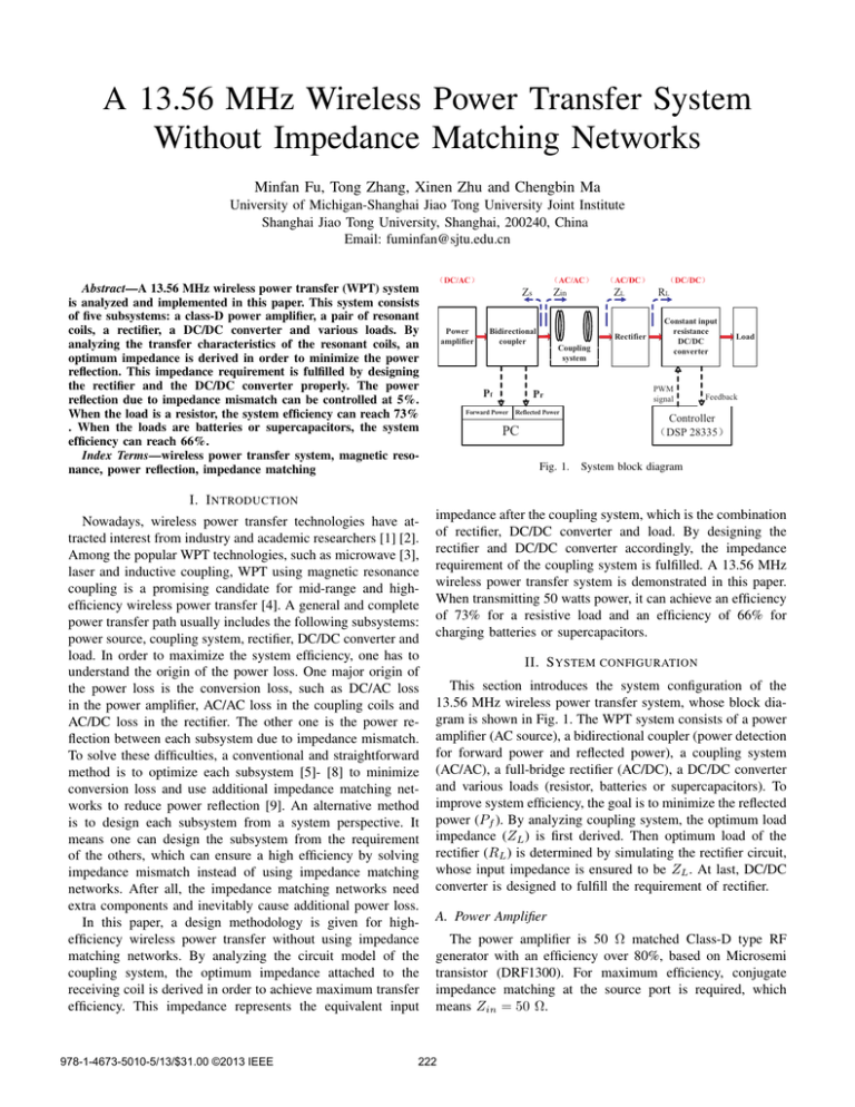
A 13.56 MHz Wireless Power Transfer System Without Impedance Matching Networks Minfan Fu, Tong Zhang, Xinen Zhu and Chengbin Ma University of Michigan-Shanghai Jiao Tong University Joint Institute Shanghai Jiao Tong University, Shanghai, 200240, China Email: fuminfan@sjtu.edu.cn Abstract—A 13.56 MHz wireless power transfer (WPT) system is analyzed and implemented in this paper. This system consists of five subsystems: a class-D power amplifier, a pair of resonant coils, a rectifier, a DC/DC converter and various loads. By analyzing the transfer characteristics of the resonant coils, an optimum impedance is derived in order to minimize the power reflection. This impedance requirement is fulfilled by designing the rectifier and the DC/DC converter properly. The power reflection due to impedance mismatch can be controlled at 5%. When the load is a resistor, the system efficiency can reach 73% . When the loads are batteries or supercapacitors, the system efficiency can reach 66%. Index Terms—wireless power transfer system, magnetic resonance, power reflection, impedance matching ˄DC/AC˅ ˄AC/AC˅ Zs Power amplifier Zin Bidirectional coupler ˄AC/DC˅ ZL Rectifier Coupling system Pf Pr Forward Power Reflected Power PC Fig. 1. ˄DC/DC˅ RL Constant input resistance DC/DC converter PWM signal Load Feedback Controller ˄DSP 28335˅ System block diagram I. I NTRODUCTION Nowadays, wireless power transfer technologies have attracted interest from industry and academic researchers [1] [2]. Among the popular WPT technologies, such as microwave [3], laser and inductive coupling, WPT using magnetic resonance coupling is a promising candidate for mid-range and highefficiency wireless power transfer [4]. A general and complete power transfer path usually includes the following subsystems: power source, coupling system, rectifier, DC/DC converter and load. In order to maximize the system efficiency, one has to understand the origin of the power loss. One major origin of the power loss is the conversion loss, such as DC/AC loss in the power amplifier, AC/AC loss in the coupling coils and AC/DC loss in the rectifier. The other one is the power reflection between each subsystem due to impedance mismatch. To solve these difficulties, a conventional and straightforward method is to optimize each subsystem [5]- [8] to minimize conversion loss and use additional impedance matching networks to reduce power reflection [9]. An alternative method is to design each subsystem from a system perspective. It means one can design the subsystem from the requirement of the others, which can ensure a high efficiency by solving impedance mismatch instead of using impedance matching networks. After all, the impedance matching networks need extra components and inevitably cause additional power loss. In this paper, a design methodology is given for highefficiency wireless power transfer without using impedance matching networks. By analyzing the circuit model of the coupling system, the optimum impedance attached to the receiving coil is derived in order to achieve maximum transfer efficiency. This impedance represents the equivalent input 978-1-4673-5010-5/13/$31.00 ©2013 IEEE impedance after the coupling system, which is the combination of rectifier, DC/DC converter and load. By designing the rectifier and DC/DC converter accordingly, the impedance requirement of the coupling system is fulfilled. A 13.56 MHz wireless power transfer system is demonstrated in this paper. When transmitting 50 watts power, it can achieve an efficiency of 73% for a resistive load and an efficiency of 66% for charging batteries or supercapacitors. II. S YSTEM CONFIGURATION This section introduces the system configuration of the 13.56 MHz wireless power transfer system, whose block diagram is shown in Fig. 1. The WPT system consists of a power amplifier (AC source), a bidirectional coupler (power detection for forward power and reflected power), a coupling system (AC/AC), a full-bridge rectifier (AC/DC), a DC/DC converter and various loads (resistor, batteries or supercapacitors). To improve system efficiency, the goal is to minimize the reflected power (Pf ). By analyzing coupling system, the optimum load impedance (ZL ) is first derived. Then optimum load of the rectifier (RL ) is determined by simulating the rectifier circuit, whose input impedance is ensured to be ZL . At last, DC/DC converter is designed to fulfill the requirement of rectifier. A. Power Amplifier The power amplifier is 50 Ω matched Class-D type RF generator with an efficiency over 80%, based on Microsemi transistor (DRF1300). For maximum efficiency, conjugate impedance matching at the source port is required, which means Zin = 50 Ω. 222 Fig. 2. (¡) Coupling system Fig. 4. Zin C + Zs L-Lm L-Lm C Under the resonance condition (jwL + + R Γ6 Fig. 3. Zin = R + ZL Lm Vs R - w2 L2m . ZL + R Zin = Zs∗ . Equivalent circuit model for the coupling system B. Coupling system The coupling system in Fig. 2 consists of two identical helical open circuit coils. The resonance is achieved by its self-inductance and parasitic capacitance. Therefore, no external lumped capacitor is needed. The coupling system is represented by its equivalent circuit model shown in Fig. 3, in which L is the self-inductance, C is the parasitic capacitance, R is the parasitic resistance and Lm is the mutual inductance. All the circuit model parameters are given in Table I. With the help of circuit model, several parameters of the coupling system can be derived. The input impedance of the coupling system is Zin = 1 jwC 1 jwC )(ZL + R + jwL + ZL + R + jwL + 1 jwC ) 1 jwC TABLE I C OUPLING SYSTEM CIRCUIT PARAMETERS Inductance L [µH] Capacitance C [pF] Internal resistance R [Ω] Mutual inductance Lm [µH] Characteristic impedance Z0 [Ω] Source impedance Zs [Ω] Coil diameter [mm] Coils gap [mm] 7.8 17.6 3.4 0.7 50 50 320 150 = 0), (2) The maximum transfer efficiency requires no power reflection at the transmitting side, i.e. Γin = Γ∗s , which equally means ΓLQ (R + jwL + Transfer efficiency for different ZL + w2 L2m . (1) (3) For a specific coupling system, which means that L, C and R are known. When the transfer distance is fixed, which means Lm is fixed. If the source impedance is predefined, for maximum efficiency, the only controllable variable is ZL . In this paper, ZS is 50 Ω. Combining Eq. 2 and Eq. 3, it gives ZL = w2 L2m − R. 50 − R (4) Taking the parameters in Table I into Eq. 4, the calculated optimum value for ZL is 73 Ω. By sweeping ZL , the transfer efficiency curve is shown in Fig. 4. C. Rectifier At the receiving part of the coupling coils, a rectifier is used to convert AC power to DC. Usually, a full-bridge topology is used. However, most high power diodes are incapable in a 13.56 MHz system because of their low switching speed. In this paper, SiC diodes (STPSC406) are used to build a full-bridge rectifier with ceramic capacitors as the low-pass filter. The design target here is to find the optimum value of the rectifier load (RL in Fig. 1) which minimizes the power reflection. Because of the non-linearity of the diodes, it is difficult to derive the system transfer characteristics like the coupling system. Instead, the rectifier is analyzed in a commercially available simulation package, Advance Design System (ADS) by Agilent Technologies. By sweeping the load resistance in Fig. 5, the system efficiency curve and power reflection coefficient are plotted in Fig. 6. The simulation results show that when the load 223 Rin resistance equals to 95 Ω, a maximum efficiency of 76% can be achieved, and the power reflection can be reduced to 5%. In the impedance analysis for coupling system, it is required that ZL = 73 Ω, which is the input impedance of the rectifier. However when RL = 95 Ω, ZL equals to (55-27*j) Ω, which means the mismatch between rectifier and coupling system cannot be completely resolved by adjusting RL . If an ideal impedance matching network is added to tune ZL from (55-27*j) Ω to 73 Ω in ADS, the system efficiency can be improved from 76% to 81%. However when the impedance matching network is simulated using practical inductor and capacitor model, the system efficiency drops to 78%. Because impedance matching networks require extra components and will inevitably cause power loss, it is a trade-off between system efficiency and system complexity. In this paper, a wireless power transfer without impedance matching networks is proposed. HARMONIC BALANCE Diode model D406 Is=10.000e-21 Rs=0.18245 N=0.70243 Cjo=190.97e-12 Vj=0.96959 M=0.44869 Fc=0.5 Isr=15.036e-9 Nr=4.9950 Ikf=185.81 Ibv=1e-10 Nbv=1e-10 Xti=2 Eg=3.26 Tnom=27 Allow Scaling=no S2P file for coupling system + Vbf S1 PWM1 Load Buck Fig. 7. Cascade Boost-Buck converter Iin D1=D406 D2=D406 Vout S2 PWM2 Boost LSSP Vin Vbf Verr=Vin-Iin*Rref Vref=Vbf-Vin*k Verr>0 Vref>0 Yes No Yes No RL Z=50 ¡ 4.7 nF 4.7 nF - Increase PWM1 D3=D406 D4=D406 Fig. 5. Increase PWM2 Reduce PWM2 Control block for the DC/DC converter Simulation setup A DC/DC converter serves as a bridge between the load and the rectifier. It serves to convert the output DC voltage from rectifier to another DC voltage level, which suits the load voltage requirement. Actually, it can also convert the load impedance to another value, which is the input impedance of the DC/DC converter. Thus a DC/DC converter can be used to achieve the optimum value of RL in a WPT system. A cascaded Boost-Buck converter is used in this paper, whose topology is shown in Fig. 7. It is a combination of two classical DC/DC converters (boost and buck) in power electronics. The control method is shown in Fig. 8. By controlling the ratio of the input voltage (Vin ) to the input current (Iin ), the input resistance value can be controlled at Rref . Vbf represents the ˄¡˅ Reduce PWM1 Fig. 8. D. DC/DC converter Fig. 6. Iin Vin ˄¡˅ System efficiency and reflection coefficient for different RL voltage of the buffer capacitor. In order to make sure boost converter can work and the power conservation is satisfied. Vbf should be controlled at a constant value, which is higher than Vin , i.e. k (refer to Fig. 8) should be larger than one. III. E XPERIMENTS RESULTS The experiment setup is shown in Fig. 9, which includes all the subsystems described above. In the following experiments, the setup of the DC/DC controller is Rref = 100 Ω and k = 1.2, which means Rin is controlled at 100 Ω and Vbf is controlled at 1.2*Vin in Fig. 7. And the forward power (Pf in Fig. 1) is 50 watts. The system efficiency is defined as the ratio of the power absorbed by the load to the forward power. When the load is an electrical load, by sweeping the load resistance, the input resistance of the DC/DC is maintained at 100 Ω to keep track with the optimum operation condition and minimize the system power reflection. Fig. 10 shows the system efficiency and power reflection coefficient. When the load is batteries or supercapacitors, whose terminal voltage rises during the charging process. It means the final load impedance changes over time. The charging efficiency for batteries is 67% and that for supercapacitors is 66%. It shows that the system can work at a stable condition even for large load impedance variation. 224 Fig. 9. [6] X. Liu and S.Y.R.Hui, ”Equivalent circuit modeling of a multilayer planar winding array structure for use in a universal contactless battery charging platform,” IEEE Transactions on Power Electronics, vol. 22, no. 1, pp. 21-29, Jan. 2007. [7] B. Cannon, J. Hoburg, D. Stancil, and S. Goldstein, ”Magnetic resonant coupling as a potential means for wireless power transfer to multiple small receivers,” IEEE Trans. Power Electron., vol. 24, no. 7, pp. 1819C1825, Jul. 2009. [8] W. Chen, R. A. Chinga, S. Yoshida, J. Lin, C. Chen and W. Lo, ”A 25.6 W 13.56 MHz Wireless Power Transfer System with a 94% Efficiency GaN Class-E Amplifier,” Microwave Symposium Digest, pp. 1-3, June 2012 [9] T.Beh, M.Kato, T.Imura, S.Oh, Y.Hori, ”Automated Impedance Matching System for Robust Wireless Power Transfer via Magnetic Resonance Coupling,” Industrial Electronics, IEEE Transactions on, Volume: pp, Issue99, June 2012. System configuration ¡ Fig. 10. System efficiency and reflection coefficient IV. C ONCLUSION In this paper, a high-efficiency 13.56 MHz wireless power transfer system is demonstrated without using impedance matching network. The power reflection due to impedance mismatch can be greatly reduced by deriving the requirement of each subsystem and properly designing them from a system perspective. This system can supply power for various loads. The system efficiency can achieve 73% when load is resistor and 66% when charging batteries or supercapacitors. R EFERENCES [1] H. Jabbar, Y. Song, T.Jeong, ”RF energy harvesting system and circuits for charging of mobile devices,” Consumer Electronics, IEEE Transactions on , vol.56, no.1, pp. 247-253, February 2010 [2] Sai Chun Tang, F. Jolesz, G. Clement, ”A wireless batteryless deep-seated implantable ultrasonic pulser-receiver powered by magnetic coupling,” Ultrasonics, Ferroelectrics and Frequency Control, IEEE Transactions on, vol.58, no.6, pp. 1211-1221, June 2011 [3] W. C. Brown, ”The history of power transmission by radio waves,” IEEE Trans. Microw. Theory Tech., vol. MTT-32, no. 9, pp. 1230-1242, Sep. 1984. [4] A. Kurs, A. Karalis, R. Moffatt, J. D. Joannopoulos, P. Fisher, and M. Soljacic, ”Wireless power transfer via strongly coupled magnetic resonances,” Science Express, vol. 317, pp. 83-86, July 2007. [5] Imura, T.; Hori, Y., ”Maximizing Air Gap and Efficiency of Magnetic Resonant Coupling for Wireless Power Transfer Using Equivalent Circuit and Neumann Formula,” Industrial Electronics, IEEE Transactions on, vol.58, no. 10, pp. 4746-4752, Oct. 2011 225


