ARTICLES
PUBLISHED ONLINE: 24 MARCH 2013 | DOI: 10.1038/NPHOTON.2013.32
Single-nanowire solar cells beyond the
Shockley–Queisser limit
Peter Krogstrup1† *, Henrik Ingerslev Jørgensen2†, Martin Heiss3†, Olivier Demichel3, Jeppe V. Holm2,
Martin Aagesen2, Jesper Nygard1 and Anna Fontcuberta i Morral3 *
Light management is of great importance in photovoltaic cells, as it determines the fraction of incident light entering the
device. An optimal p–n junction combined with optimal light absorption can lead to a solar cell efficiency above the
Shockley–Queisser limit. Here, we show how this is possible by studying photocurrent generation for a single core–shell
p–i–n junction GaAs nanowire solar cell grown on a silicon substrate. At 1 sun illumination, a short-circuit current of
180 mA cm–2 is obtained, which is more than one order of magnitude higher than that predicted from the Lambert–Beer
law. The enhanced light absorption is shown to be due to a light-concentrating property of the standing nanowire, as
shown by photocurrent maps of the device. The results imply new limits for the maximum efficiency obtainable with III–V
based nanowire solar cells under 1 sun illumination.
N
anowire-based solar cells hold great promise for third-generation photovoltaics and for powering nanoscale devices1,2.
With the advent of third-generation photovoltaics, solar
cells will become cheaper and more efficient than current devices.
In particular, a cost reduction may be achieved by reducing material
use through the fabrication of nanowire arrays and radial p–n junctions3–5. The geometry of nanowire crystals is expected to favour
elastic strain relaxation, providing great freedom in the design of
new compositional multijunction solar cells6 grown on mismatched
materials7,8. The efficiencies of nanostructured solar cells have
increased over time and have now reached up to 13.8%, due to
improvements in materials and new device concepts9–14.
Light absorption in standing nanowires is a complex phenomenon, with a strong dependence on nanowire dimensions and the
absorption coefficient of the raw materials15–18. In low-absorbing
microwire arrays, such as those composed of silicon, light absorption is understood via ray optics or by calculation of the integrated
local density of optical states of the nanowire film19,20. Interestingly,
when these arrays stand on a Lambertian back-reflector, an asymptotic increase in light trapping for low filling factors (FFs) is
predicted19. This is advantageous for improvement of the efficiency-to-cost ratio of solar cells and has led to the demonstration
of microwire arrays exhibiting higher absorption than in the equivalent thickness of textured film19,21,22. The case for nanowires is
quite different. Nanowire diameters are smaller than or comparable
to the radiation wavelength. In this case, optical interference and
guiding effects play a dominant role in relation to reflectivity and
absorption spectra. For low-absorbing materials (for example, indirect bandgap materials such as silicon), waveguiding effects plays a
key role23,24, whereas highly absorbing semiconductors (such as
direct-bandgap GaAs) exhibit resonances that increase the total
absorption several times. Nanowires lying on a substrate also
exhibit such resonances, often described by Mie theory25,26,
although the total absorption rate is significantly lower27,28. Even
though the optical absorption of nanowires arranged in an array
has been shown to be far more complex than in thin films, nanowire
vertical arrays currently seem to be the most reasonable device proposal. One elegant device consists of a single standing nanowire
solar cell, contacted on top by a transparent electrode and at the
bottom through the substrate. Although the characterization of
single nanowires lying on a substrate is quite common, to date
there have been no studies on single standing nanowires.
In this Article, we present experimental measurements on single
GaAs nanowire solar cells, as grown on a silicon substrate, where
the p-section is contacted through a highly doped substrate and
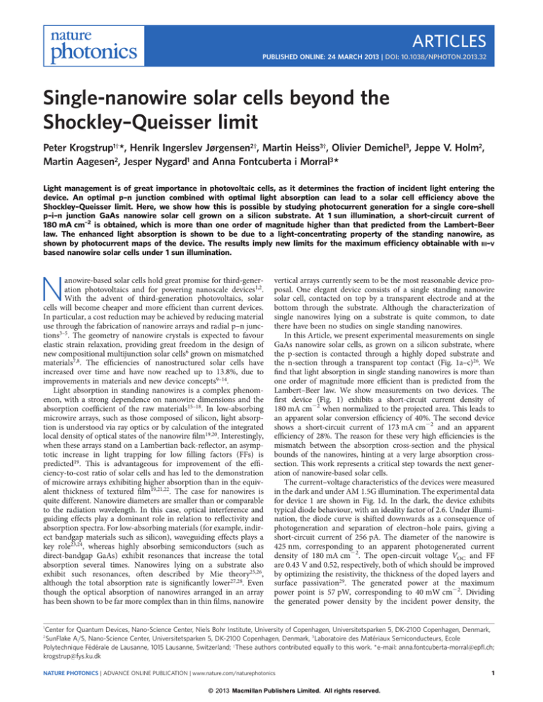
the n-section through a transparent top contact (Fig. 1a–c)26. We
find that light absorption in single standing nanowires is more than
one order of magnitude more efficient than is predicted from the
Lambert–Beer law. We show measurements on two devices. The
first device (Fig. 1) exhibits a short-circuit current density of
180 mA cm22 when normalized to the projected area. This leads to
an apparent solar conversion efficiency of 40%. The second device
shows a short-circuit current of 173 mA cm22 and an apparent
efficiency of 28%. The reason for these very high efficiencies is the
mismatch between the absorption cross-section and the physical
bounds of the nanowires, hinting at a very large absorption crosssection. This work represents a critical step towards the next generation of nanowire-based solar cells.
The current–voltage characteristics of the devices were measured
in the dark and under AM 1.5G illumination. The experimental data
for device 1 are shown in Fig. 1d. In the dark, the device exhibits
typical diode behaviour, with an ideality factor of 2.6. Under illumination, the diode curve is shifted downwards as a consequence of
photogeneration and separation of electron–hole pairs, giving a
short-circuit current of 256 pA. The diameter of the nanowire is
425 nm, corresponding to an apparent photogenerated current
density of 180 mA cm22. The open-circuit voltage VOC and FF
are 0.43 V and 0.52, respectively, both of which should be improved
by optimizing the resistivity, the thickness of the doped layers and
surface passivation29. The generated power at the maximum
power point is 57 pW, corresponding to 40 mW cm22. Dividing
the generated power density by the incident power density, the
1
Center for Quantum Devices, Nano-Science Center, Niels Bohr Institute, University of Copenhagen, Universitetsparken 5, DK-2100 Copenhagen, Denmark,
SunFlake A/S, Nano-Science Center, Universitetsparken 5, DK-2100 Copenhagen, Denmark, 3 Laboratoire des Matériaux Semiconducteurs, Ecole
Polytechnique Fédérale de Lausanne, 1015 Lausanne, Switzerland; † These authors contributed equally to this work. * e-mail: anna.fontcuberta-morral@epfl.ch;
krogstrup@fys.ku.dk
2
NATURE PHOTONICS | ADVANCE ONLINE PUBLICATION | www.nature.com/naturephotonics
© 2013 Macmillan Publishers Limited. All rights reserved.
1
ARTICLES
NATURE PHOTONICS
absorption is through the concept of an absorption cross-section.
The absorption cross-section is defined as Aabs ¼ ah, where a is the
physical cross-section of the nanowire and h is the absorption efficiency. It is largely accepted that the absorption cross-section in
nanoscale materials is larger than their physical size. In systems
such as quantum dots, the absorption cross-section can exceed the
physical size by a factor of up to 8 (ref. 33). We calculated the absorption cross-section of the nanowires as a function of the nanowire
diameter and incident wavelength (Fig. 2b). The absorption crosssection is, in all cases, larger than the physical cross-section of the
nanowire. It is interesting to note that the absorption of photons
from an area larger than the nanowire itself is equivalent to a builtin light concentration C. Light concentration has an additional
benefit in that it increases the open-circuit voltage with a term
kT ln C, thereby increasing the efficiency34–36. The largest absorption
cross-section in Fig. 2b is 1.13 × 10⁶ nm2 for a nanowire diameter
of 380 nm (a ¼ 9.38 × 10⁴ nm2), corresponding to an overall builtin light concentration of 12.
Measurements of the external quantum efficiency (EQE) normalized by the physical area for both lying and standing nanowire
devices are shown in Fig. 3a (see Supplementary Section S1 for
a
ITO
SU-8
d - SiO 2 on
Si - p-dope
b
top
c 5 µm
n-type,
Si doped
0.5 µm
Undoped
p-type,
Be doped
0.5 µm
d
Current (pA)
ISC = 256 pA (180 mA cm−2)
VOC = 0.43 V
FF = 0.52
300
a
200
0.2
0.3
0.4
14
900
12
800
10
700
8
600
6
500
4
400
2
Wavelength (nm)
−0.2
0
−0.1 0.0 0.0 0.1
1,000
0.5
−100
300
−200
0
100
AM 1.5
−300
200
300
Diameter (nm)
400
Geometric cross-section area (µm2)
0.050
0.100
0.150
0.005
0.020
b
1,100
Cross-section
1.0
1,000
Wavelength (nm)
900
0.8
800
0.6
700
600
0.4
500
solar cell yields an apparent efficiency of 40%. To understand the
extreme photon collection boost in free-standing single GaAs nanowires, we used a finite-difference time-domain (FDTD) method to
model a 2.5-mm-long nanowire embedded in SU-8 as a function
of its diameter and of the wavelength of the plane-wave radiation propagating along the nanowire axis30–32. Figure 2a shows the wavelength
and diameter dependence of the absorption rate of such a nanowire.
Note that the absorption is zero for wavelengths larger than 900 nm
where the absorption coefficient of GaAs goes to zero. Two dominant
branches for low and high diameters are observed, corresponding to
resonances similar to the Mie resonances observed in nanowires
lying on a substrate25. Light absorption in the standing nanowire is
enhanced by a factor of between 10 and 70 with respect to the equivalent thin film. Another way to express this enhancement in
2
0.2
400
300
Absorption cross-section area (µm2)
Figure 1 | Electrical characterization of a single nanowire solar cell (device 1).
a, Schematic of the vertical single-nanowire radial p–i–n device connected to a
p-type doped silicon wafer by epitaxial growth. b, Left: doping structure of the
nanowire. The p-type doped core is in contact with the doped silicon substrate
and the n-type doped shell is in contact with the ITO. Right: Scanning electron
microscope (SEM) image of a nanowire solar cell before adding the top
contact, with a 308 angle from the vertical. c, SEM images of the device seen
from the top electrode. The nanowire is 2.5 mm high and has a diameter of
425 nm. d, Current–voltage characteristics of the device in the dark and
under AM 1.5G illumination, showing the figure-of-merit characteristics.
AM 1.5G absorption rate (J−1 s−1)
Dark
−0.3
×1027
1,100
Absorption rate
100
Voltage (V)
DOI: 10.1038/NPHOTON.2013.32
0.0
100
200
300
Diameter (nm)
400
Figure 2 | Optical simulations of a single nanowire solar cell.
a,b, Simulations of light absorption in a 2.5 mm standing GaAs nanowire that
is fully embedded in SU-8 (n ¼ 1.67) on a silicon substrate: the absorption
rate of solar AM 1.5G radiation (a) and simulated absorption cross-section
(b) exhibit two main resonant branches, similar to Mie resonances observed
in nanowires lying on a substrate. The periodic modulation with wavelength
is a result of Fabry–Pérot interference in the polymer layer and not an
artefact of the simulation.
NATURE PHOTONICS | ADVANCE ONLINE PUBLICATION | www.nature.com/naturephotonics
© 2013 Macmillan Publishers Limited. All rights reserved.
NATURE PHOTONICS
0.02
a 15
Apparent EQE (considering projected area)
ARTICLES
DOI: 10.1038/NPHOTON.2013.32
Vertical 0.142
projected
b
µm2
10
5
Horizontal
0.97 µm2 projected
1 µm
488 nm
0
500
600
700
800
0
900
Wavelength (nm)
0.06
0.18
c
d
676 nm
1 µm
1 µm
800 nm
0
0
Figure 3 | Optical characterization of a single nanowire solar cell (device 2). a, EQE normalized by indicated projected area, comparing vertical and
horizontal nanowire solar cells. For the vertical standing solar cell, a 15-fold increase in photon collection is obtained close to the bandgap. EQE becomes
negligible for photon wavelengths below the bandgap of GaAs, meaning that there is no contribution from absorption in the silicon substrate45. b–d, Scanning
photocurrent measurements on our single vertical nanowire device for three different excitation laser wavelengths, normalized to the incident photon flux.
Scale bar, 1 mm.
more details). Lying nanowires exhibit EQE values up to 2 due to
Mie resonances37, while for standing nanowires values of up to
14.5 are reached. This further confirms that the absorption
cross-section is several times larger than the apparent crosssection of the wire, especially at wavelengths close to the bandgap.
To further understand the absorption boost in our devices, we
spatially mapped the photocurrent generated by a vertical nanowire
device for three different excitation wavelengths: 488 nm, 676 nm
and 800 nm. The results presented in Fig. 3b–d are deconvoluted
with the point-spread function of the diffraction-limited laser spot.
As seen in the figure, a photocurrent from an area much larger
than the size of the laser spot appears for all three wavelengths. A
fit to the data allows the estimation of an effective absorption crosssection diameter of 1.2 mm (488 nm), 1.0 mm (676 nm) and 1.3 mm
(800 nm), respectively. Hence, the absorption boost in our device is
due to an unexpectedly large absorption cross-section of the vertical
nanowire geometry. This is equivalent to a built-in light concentration
of 8, which is in good agreement with our theoretical predictions. In
addition, we speculate that the top-contact geometry further contributes to the resonant absorption effect, thereby increasing the absorption cross-section and the boost in photogenerated current.
Finally, we put our results into perspective by comparing them to
the best existing technologies and to the design principles for
increasing efficiency. In Table 1 we list the best values for leading
technologies such as single-junction crystalline silicon (c-Si) and
GaAs, as well as triple-junction devices. The highest efficiency is
provided by the triple-junction solar cell (34.1%), with a shortcircuit current of 14.7 mA cm22. In this case the short-circuit
current is kept relatively low as it has to be matched between the
three cells connected in series, and it is the high efficiency that generates the increase in VOC. The highest short-circuit current is
obtained in the c-Si solar cell, where light management techniques
result in a boost in the photogenerated current of 42.7 mA cm22.
The record efficiency recorded by Alta Devices with GaAs was
obtained with a relatively thin film (a few micrometres, rather
than a few hundred micrometres as in standard cells). This brings
us to the discussion of what determines high efficiency. A solar
cell operates at a voltage that maximizes the generated power, dictated by the short-circuit current, FF and VOC. Designing with a
view to achieving higher efficiencies requires strategies for increasing these values38,39. Improving the first two parameters – shortcircuit current and FF – mainly involves device ‘engineering’,
while obtaining the ultimate VOC is dictated by the thermodynamics
of solar energy conversion into electrical work. Within the
Shockley–Queisser model, VOC is limited as follows36:
Voc =
Eg
T
kT
V
4n2
ln emit + ln
1−
− ln QE
−
Tsun
q
q
Vsun
C
where T and Tsun are the temperatures of the cell and the sun,
respectively, Vemit and Vsun correspond to the solid angle of
NATURE PHOTONICS | ADVANCE ONLINE PUBLICATION | www.nature.com/naturephotonics
© 2013 Macmillan Publishers Limited. All rights reserved.
3
ARTICLES
NATURE PHOTONICS
DOI: 10.1038/NPHOTON.2013.32
Table 1 | JSC , FF, VOC , area and efficiency of the best photovoltaic technologies compared with the standing nanowire
configuration presented in this work.
Technology
c-Si
GaAs
Triple junction
This work
J SC (mA cm22)
42.7
29.68
14.57
180
FF (%)
82.8 (ref. 47)
86.5
86.0
52
VOC (V)
0.706
1.122
3.014
0.43
Area (cm2)
4
1
30
1.42 × 1029
h (%)
25.0
28.8 (ref. 48)
37.7
40*
The low VOC and FF values indicate the potential for improvement of the nanowire cell presented. See main text for discussion.
*Apparent efficiency calculated with the projected area of the cell.
emission and collection, n is the refractive index of the material, and
QE is the emission quantum efficiency. The first term is related to
the Carnot efficiency, which reduces VOC by 5%. The second
term corresponds to the entropic losses occurring during work generation. The first entropy loss is due to non-reciprocity in the angle
of light absorption and emission. Light-resonant structures such as
nanowires can reduce the contribution of this term36. The second
entropy loss takes account of the concentration factor, given by
the refractive index and any external concentration: VOC increases
by implementing light-trapping strategies, with the additional
benefit of increasing absorption close to the bandgap40,41. The last
entropic term refers to non-radiative losses. It can be reduced to
zero by increasing QE to 1. The impressive result for GaAs cells
achieved by Alta Devices was obtained thanks to increasing the
QE in a GaAs thin film to 1. Our results provide a further path
for higher-efficiency solar cells. Even though the electrical characteristics shown are not yet ideal, we observe a light concentration effect
plus a significant increase in absorption rate close to the bandgap,
similar to that proposed in ref. 36. These two effects are such that
nanowire structures can reduce the entropy in the conversion of
solar energy into electrical work, thereby providing a path for
increasing the efficiency of solar cells. It is also important to note
that the unexpected increase in the absorption cross-section
enables nanowires to be further separated from one another, resulting in major cost reductions for the final device. Our experiments
indicate that a good interwire distance would be 1.2 mm. A nanowire solar cell consisting of nanowires similar to the device shown in
Fig. 1, positioned in a hexagonal array with a pitch of 1 mm (optical
cross-section with a diameter of 1.2 mm), would have an optical
FF of 1, and it would only use a material volume equivalent to
that of a 546 nm film and exhibit a conversion efficiency of 4.6%.
By using devices with a smaller area (see left branch in Fig. 2a,b),
one could further reduce the amount of material used by a factor
of up to 72. By improving the electrical characteristics of the p–n
junction, higher efficiencies could be obtained. By considering an
effective light concentration of only 15, an array of GaAs nanowires
with ideal characteristics would exhibit an efficiency of 33.4%,
thereby overcoming the Shockley–Queisser limit for planar GaAs
solar cells illuminated by 1.5 AM radiation, according to the discussion presented in the foregoing text34,42. Even higher efficiencies
could be achieved if the device design were tailored for higher
light concentrations and QE. Note that axial junctions, which
have the same junction area as the projected area, would obtain
the full benefit from such a concentrator effect, and it would be
possible to directly compare the performance of GaAs nanowire
solar cells under 1 sun with planar GaAs cells under 10 suns. We
demonstrate here that single-nanowire devices generate severalfold higher power than their projected areas suggest when they
are standing upright, a configuration that also minimizes their footprint. It should be noted that if one were to build a single-nanowire
solar cell, then a flat-lying nanowire would exhibit 15 times lower
power density compared to the standing nanowire device due to the
light concentration effect. This enhancement in energy conversion
at the nanoscale will make standing nanowires useful as energy harvesters, with minimum footprint, for feeding other devices on the
4
same chip. This is already the case for nanowire-based p–n junctions
with non-ideal characteristics such as the one demonstrated in this
work. Last, but not least, the improvement in photon collection
renders them (in general) ideal for use as photodetectors.
In conclusion, we have observed a remarkable boost in absorption in single-nanowire solar cells that is related to the vertical configuration of the nanowires and to a resonant increase in the
absorption cross-section. These results open a new route to thirdgeneration solar cells, local energy harvesters on nanoscale devices
and photon detectors.
Methods
Nanowire growth. Nanowires were grown on oxidized Si(111) with 100 nm
apertures using a self-catalysed method. The gallium nominal growth rate was
900 nm h21, the substrate temperature was 630 8C and the V/III ratio was 4 (refs
43,44). The p-doping of the core was achieved by adding a flux of beryllium during
axial growth45. Cores were annealed for 10 min at 630 8C. The shell was obtained
at 465 8C, a growth rate of 300 nm h21 and with a V/III ratio of 50. The n-type
doping was obtained by adding silicon to the growth step46.
Device fabrication and characterization. SU-8 was spun onto the substrate at
4,000 r.p.m. for 45 s and cured with 1 min ultraviolet light and 3 min on a hotplate
at 185 8C. An etch-back with a 1–3 min oxygen plasma etch was then performed to
free the nanowire tip. The top contact was defined by electron-beam lithography
followed by evaporation of indium tin oxide (ITO) (for more details see
Supplementary Section S1). The bottom contact was obtained by silver gluing to the
back-side of the wafer. Current–voltage characteristics were measured in the dark
and under 1.5 G conditions with a standard solar simulator (LOT – Oriel 150 W
xenon lamp) with a 1-inch beam diameter and an AM 1.5G filter. A photocurrent
map of the devices was collected by scanning the contacted sample under the
laser spot focused with a ×63 and 0.75 NA lens.
FDTD method simulations. The absorption of standing 2.5 mm GaAs nanowires
of different diameters, standing on silicon and surrounded by SU-8, was calculated
by solving Maxwell equations in three dimensions for an incident plane-wave
radiation normal to the substrate. The wave equation was solved in the time domain
according to refs 30 and 27.
Received 6 November 2012; accepted 28 January 2013;
published online 24 March 2013
References
1. Tian, B. Z. et al. Coaxial silicon nanowires as solar cells and nanoelectronic
power sources. Nature 449, 885–888 (2007).
2. Law, M., Greene, L. E., Johnson, J. C., Saykally, R. & Yang, P. D. Nanowire
dye-sensitized solar cells. Nature Mater. 4, 455–459 (2005).
3. Kayes, B. M., Atwater, H. A. & Lewis, N. S. Comparison of the device physics
principles of planar and radial p–n junction nanorod solar cells. J. Appl. Phys.
97, 114302 (2005).
4. Spurgeon, J. M. et al. Flexible, polymer-supported, Si wire array photoelectrodes.
Adv. Mater. 22, 3277–3281 (2010).
5. Fan, Z. et al. Three-dimensional nanopillar-array photovoltaics on low-cost and
flexible substrates. Nature Mater. 8, 648–653 (2009).
6. Kempa, T. J. et al. Single and tandem axial p–i–n nanowire photovoltaic devices.
Nano Lett. 8, 3456–3460 (2008).
7. Chuang, L. C. et al. Critical diameter for III–V nanowires grown on
lattice-mismatched substrates. Appl. Phys. Lett. 90, 043115 (2007).
8. Glas, F. Critical dimensions for the plastic relaxation of strained axial
heterostructures in free-standing nanowires. Phys. Rev. B 74, 121302 (2006).
9. Tsakalakos, L. et al. Silicon nanowire solar cells. Appl. Phys. Lett. 91,
233117 (2007).
10. Goto, H. et al. Growth of core–shell InP nanowires for photovoltaic application
by selective-area metal organic vapor phase epitaxy. Appl. Phys. Express 2,
035004 (2009).
NATURE PHOTONICS | ADVANCE ONLINE PUBLICATION | www.nature.com/naturephotonics
© 2013 Macmillan Publishers Limited. All rights reserved.
NATURE PHOTONICS
ARTICLES
DOI: 10.1038/NPHOTON.2013.32
11. Garnett, E. C. & Yang, P. Silicon nanowire radial p–n junction solar cells.
J. Am. Chem. Soc. 130, 9224–9225 (2008).
12. Wallentin, J. et al. InP nanowire array solar cells achieving 13.8% efficiency by
exceeding the ray optics limit. Science 339, 1057–1060 (2013).
13. Tian, B. Z. & Lieber, C. M. Design, synthesis, and characterization of novel
nanowire structures for photovoltaics and intracellular probes. Pure Appl. Chem.
83, 2153–2169 (2011).
14. Dalmau-Mallorqui, A., Epple, F. M., Fan, D., Demichel, O. & Fontcuberta i
Morral, A. Effect of the pn junction engineering on Si microwire-array solar cells.
Phys. Status Solidi 209, 1588–1591 (2012).
15. Tsakalakos, L. et al. Strong broadband optical absorption in silicon nanowire
films. J. Nanophot. 1, 013552 (2007).
16. Zhu, J. et al. Optical absorption enhancement in amorphous silicon nanowire
and nanocone arrays. Nano Lett. 9, 279–282 (2009).
17. Mariani, G. et al. Patterned radial GaAs nanopillar solar cells. Nano Lett. 11,
2490–2494 (2011).
18. Muskens, O. L., Gomez-Rivas, J., Algra, R. E., Bakkers, E. P. A. M. &
Lagendijk, A. Design of light scattering in nanowire materials for photovoltaic
applications. Nano Lett. 8, 2638–2642 (2008).
19. Kosten, E. D., Warren, E. L. & Atwater H. A. Ray optical light trapping in silicon
microwires: exceeding the 2n 2 intensity limit. Opt. Express 19, 3316–3331 (2011).
20. Callahan, D. M., Munday, J. N. & Atwater H. A. Solar cell light trapping beyond
the ray optic limit. Nano Lett. 12, 214–218 (2012).
21. Kelzenberg, M. D. et al. Enhanced absorption and carrier collection in Si wire
arrays for photovoltaic applications. Nature Mater. 9, 239–244 (2010).
22. Diedenhofen, S. et al. Strong geometrical dependence of the absorption of light
in arrays of semiconductor nanowires. ACS Nano 5, 2316–2323 (2011).
23. Kwanyong, S. et al. Multicolored vertical silicon nanowires. Nano Lett. 11,
1851–1856 (2011).
24. Van Vugt, L. L., Zhang, B., Piccione, B., Spector, A. A. & Agarwal, R. Sizedependent waveguide dispersion in nanowire optical cavities: slowed light and
dispersionless guiding. Nano Lett. 9, 1684–1688 (2009).
25. Cao, L. et al. Engineering light absorption in semiconductor nanowire devices.
Nature Mater. 8, 643–647 (2009).
26. Brönstrup, G. et al. A precise optical determination of nanoscale diameters of
semiconductor nanowires. Nanotechnology 22, 385201 (2011).
27. Heiss, M. & Fontcuberta i Morral A. Fundamental limits in the external
quantum efficiency of single nanowire solar cells. Appl. Phys. Lett. 99,
263102 (2011).
28. Kempa, T. et al. Coaxial multishell nanowires with high-quality electronic
interfaces and tunable optical cavities for ultrathin photovoltaics. Proc. Natl
Acad. Sci. USA 109, 1407–1412 (2011).
29. Nelson, J. The Physics of Solar Cells (Imperial College, 2003).
30. Oskooi, A. F. et al. MEEP: a flexible free-software package for electromagnetic
simulations by the FDTD method. Comp. Phys. Comm. 181, 687–702 (2010).
31. Kupec, J. & Witzigmann, B. Dispersion, wave propagation and efficiency analysis
of nanowire solar cells. Opt. Express 17, 10399–10410 (2009).
32. Cao, L. Y. et al. Semiconductor nanowire optical antenna solar absorbers.
Nano Lett. 10, 439–445 (2010).
33. Leatherdale, C. A., Woo, W. K., Mikulec, F. V. & Bawendi, M. G. On the
absorption cross section of CdSe nanocrystal quantum dots. J. Phys. Chem. B
106, 7619–7622 (2002).
34. Henry, C. H. Limiting efficiencies of ideal single and multiple energy gap
terrestrial solar cells. J. Appl. Phys. 51, 4494–4500 (1980).
35. Araújo, G. L. & Marti, A. Absolute limiting efficiencies for photovoltaic energyconversion. Solar Ener. Mater. Solar Cells 33, 213–240 (1994).
36. Polman, A. & Atwater H. A. Photonic design principles for ultrahigh-efficiency
photovoltaics. Nature Mater. 11, 174–177 (2012).
37. Kempa, T. et al. Coaxial multishell nanowires with high-quality electronic
interfaces and tunable optical cavities for ultrathin photovoltaics. Proc. Natl
Acad. Sci. USA 109, 1407–1412 (2012).
38. Campbell, P. & Green, M. A. The limiting efficiency of silicon solar cells under
concentrated sunlight. IEEE Trans. Electron. Device Lett. 33, 234–239 (1986).
39. Nelson, J. The Physics of Solar Cells (Imperial College Press, 2003).
40. Luque, A. The confinement of light in solar cells. Solar Ener. Mater. 23,
152–163 (1991).
41. Yablonovitch, E. & Cody, G. D. Intensity enhancement in textured optical sheets
for solar cells. IEEE Trans. Electron. Device Lett. 29, 300–305 (1982).
42. Shockley, W. & Queisser H. J. Detailed balance limit of efficiency of p–n junction
solar cells. J. Appl. Phys. 32, 510–519 (1961).
43. Uccelli, E. et al. Three-dimensional twinning of self-catalyzed GaAs nanowires
on Si substrates. Nano Lett. 11, 3827–3832 (2011).
44. Krogstrup, P. et al. Structural phase control in self-catalyzed growth of GaAs
nanowires on silicon (111). Nano Lett. 10, 4475–4482 (2010).
45. Casadei, A. et al. Doping incorporation paths in catalyst-free Be-doped GaAs
nanowires. Appl. Phys. Lett. 102, 013117 (2013).
46. Colombo, C., Heiß, M., Graetzel, M. & Fontcuberta i Morral, A. Gallium
arsenide p–i–n radial structures for photovoltaic applications. Appl. Phys. Lett.
94, 173108 (2009).
47. Zhao, J. et al. 19.8% efficient ‘honeycomb’ textured multicrystalline and 24.4%
monocrystalline silicon solar cells. Appl. Phys. Lett. 73, 1991–1993 (1998).
48. Green, M. A., Emery, K., Hishikawa, Y., Warta, W. & Dunlop, E. D. Solar cell
efficiency tables (version 41). Prog. Photovolt. 21, 1–11 (2013).
Acknowledgements
This research was funded by the ERC starting grant UpCon and by SNF (project nos
137648, 143908) and NCCR-QSIT. A.F.i.M. thanks STI for the 2011 end-of-year fund for
MiBoots robots used in the scanning photocurrent experiment. A.F.i.M. and M.H. thank
A. Dalmau-Mallorqui and F.M. Epple for experimental support. The authors also thank
C.B. Sørensen and M.H. Madsen for assistance with MBE growth. This work was supported
by the Danish National Advanced Technology Foundation (project 022-2009-1),
a University of Copenhagen Center of Excellence, and by the UNIK Synthetic
Biology project.
Author contributions
P.K. grew the nanowire p–n junctions. H.I.J. performed I–V characterization and fabricated
the device, with help from J.V.H. and M.A. M.H. and O.D. performed the FDTD
calculations. M.H. realized the photocurrent mappings and the external quantum efficiency
measurements. A.F.i.M. and P.K. conceived and designed the experiments. A.F.i.M.,
J.N. and M.A. supervised the project. A.F.i.M., H.I.J., P.K. and M.H. composed the figures
and wrote the manuscript. All authors discussed the results and commented on
the manuscript.
Additional information
Supplementary information is available in the online version of the paper. Reprints and
permissions information is available online at www.nature.com/reprints. Correspondence and
requests for materials should be addressed to P.K. and A.F.i.M.
Competing financial interests
The authors declare no competing financial interests.
NATURE PHOTONICS | ADVANCE ONLINE PUBLICATION | www.nature.com/naturephotonics
© 2013 Macmillan Publishers Limited. All rights reserved.
5
