IC Packaging: Assembly, Types, and Advanced Techniques
advertisement

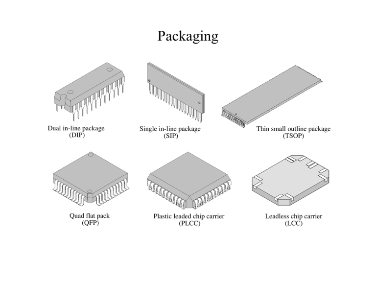
Chapter 20 Packaging Assembly and Packaging Dual in-line package (DIP) Quad flat pack (QFP) Single in-line package (SIP) Plastic leaded chip carrier (PLCC) Thin small outline package (TSOP) Leadless chip carrier (LCC) Introduction • Chips that pass the wafer sort test undergo final assembly and packaging. IC final assembly separates each good die from the wafer and attaches the die to a metal • Chips that pass the wafer sort test undergo final assembly and packaging. IC final assembly separates each good die from the wafer and a<aches the die to a metal leadframe or substrate. IC packaging encloses the die in a protec=ve package. • IC packaging performs four func=ons: protec=on from the environment/handling, signal interconnec=ons, physical support and heat dissipa=on. There are two packaging levels: -­‐ 1st level packaging involves the IC -­‐ 2nd level packaging places the IC on a circuit board. There are numerous packaging design constraints. IC final assembly consists of four steps: Backgrind -­‐ reduces the wafer thickness to the appropriate dimension. die separa=on -­‐ cuts each die from the wafer. die a<ach -­‐ the physical a<achment of the die to the leadframe or substrate. Die a<ach is done by epoxy a<ach, eutec=c a<ach and glass frit a<ach. wire bonding -­‐ a<aches fine-­‐diameter wires between die bonding pads and the terminals of the leadframe to form electrical connec=ons. The three basic types of wirebonding are: thermocompression bonding, ultrasonic bonding and thermosonic ball bonding. • Tradi=onal IC packaging materials are plas=c packaging and ceramic packaging. • Plas=c packaging uses an epoxy polymer to encapsulate the wirebonded die and leadframe. This technology has many different types of plas=c packages. • Ceramic packaging is used for state-­‐of-­‐the-­‐art IC packages that require either maximum reliability or high-­‐power. The two main types of ceramic packaging are either a refractory (high temperature) ceramic or ceramic DIP (CERDIP) technology. Both have a herme=c seal (sealed against moisture). • All assembled and packaged chips undergo a final electrical test for IC reliability. Advanced packaging designs include: Flip chip -­‐ mounts the ac=ve side of a chip toward the substrate. It uses bump technology (typically solder bumps) to form the interconnec=on between the chip and substrate. An epoxy underfill is used around the area-­‐array of bumps to improve reliability. Ball grid array (BGA) -­‐ uses a ceramic or plas=c substrate with an area array of solder balls to connect the substrate to the circuit board. To lower costs, this technology is readily integrated into standard surface mount assembly. Land Grid Array (LGA) -­‐ is a packaging technology with a square grid of contacts on the underside of a package. The contacts are to be connected to a grid of pin contacts on the PCB. Chip on board (COB) -­‐ mounts IC chips directly to the substrate, along side other surface mount (SMT) or pin-­‐ in-­‐hole (PIH) components. Tape automated bonding (TAB) -­‐ uses a plas=c tape as a chip carrier. The tape has a thin copper foil that is etched to form the leads. The chip and leads are removed from the carrier prior to assembly onto the circuit board. Mul=chip modules (MCM) -­‐ has several die assembled onto one substrate. This permits a higher density of chips. Chip scale packaging (CSP) -­‐ an IC package that is about the same size as the silicon chip (< 1.2 =mes the footprint of the die). This is a fast growing method of advanced packaging, and provides for lower cost, lower weight and lower thickness. Wafer-­‐level packaging -­‐ places the 1st level interconnec=ons and package input/output terminals on the wafer before it is diced. It is typically done with a bump interconnect process. This will simplify the IC packaging process and lower cost. LGA BGA CSP CoB MCM

