Silicon
advertisement
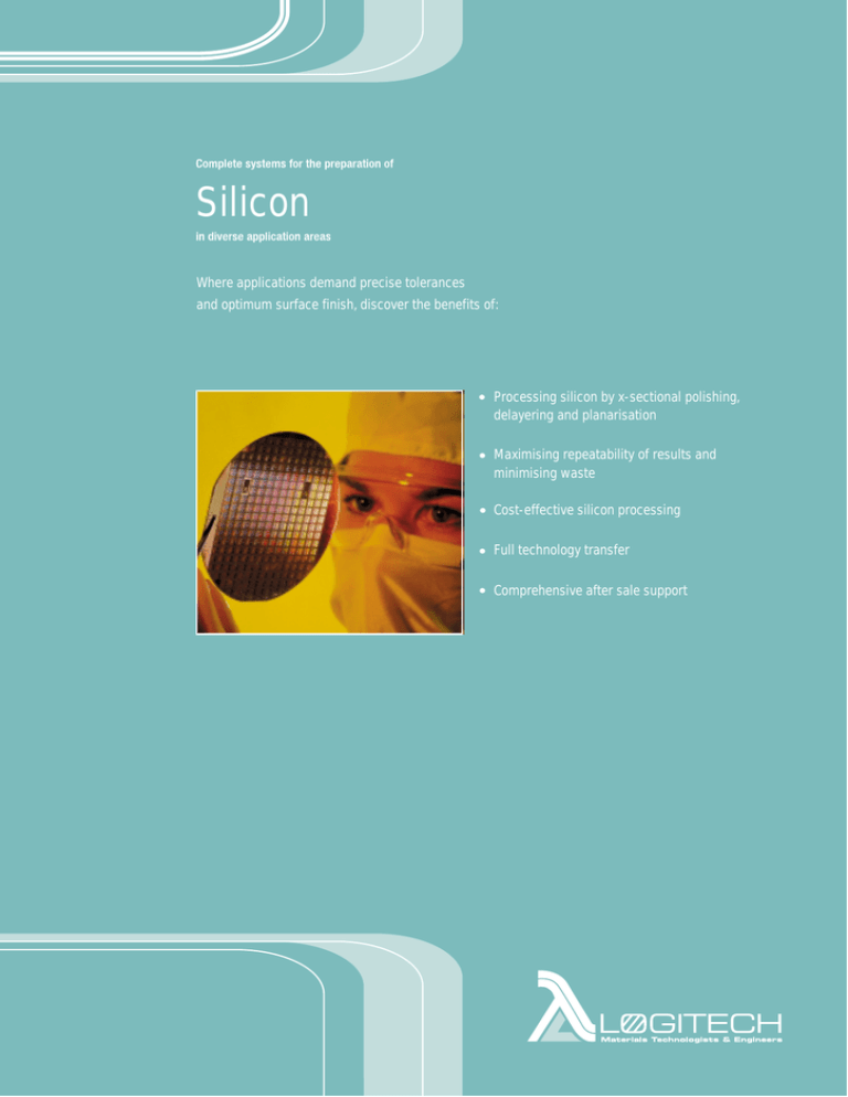
Silicon Where applications demand precise tolerances and optimum surface finish, discover the benefits of: Processing silicon by x-sectional polishing, delayering and planarisation Maximising repeatability of results and minimising waste Cost-effective silicon processing Full technology transfer Comprehensive after sale support Introduction Increasingly, R&D and production sites worldwide are realising the benefits of using Logitech precision cutting, lapping and polishing machines for accurate silicon processing. Whether for semiconductor or optical applications; for example wafer and chip manufacture or IR and polymer waveguide production, the exacting design and manufacture of standard Logitech equipment ensures the customer will achieve the highest quality results. This document provides a brief analysis of the various techniques developed by Logitech for specific silicon processes, using machines such as the APD1 and AXL1 precision saws and PM5 polishing machine. These pages highlight how your sample preparation by, for example, x-sectional polishing, backthinning, delayering or planarisation, benefits from the versatility and precision offered by the latest Logitech machine technology. Furthermore as customers continue to seek improvements in sample geometries including flatness, parallelism and surface finish, the brochure also outlines the value and customer reassurance offered by Logitech Customer Support and Technology Transfer. Application Analysis Initial discussions with the customer provide the basis for the selection of machines, special accessories and operating technology to give the best solution to particular processing problems. These discussions provide a detailed understanding of production quantity, sample dimensions, surface finish and geometric tolerance requirements. Occasionally it is necessary to have a general outline of the proposed process route but confidentiality of proprietary information is always assured. When the customer requirements have been properly analysed, Logitech can suggest the correct equipment and prepare a formal quotation for a machine system with process technology best suited to the customer’s needs. This process technology may be used in applications such as the following: • Wafer-lapping and/or polishing • Preparation of substrates for use in waveguide manufacture • Planarisation of surface layers • Cross-sectional polishing (e.g. for Physical Failure Analysis) • De-layering or face polishing Logitech’s unique consultative approach ensures that the customer achieves the best possible results using the appropriative advanced Logitech machine system. Development or Full Scale Production Logitech systems are designed to grow as quantity requirements increase. This makes it possible to start with one single workstation machine in the initial stages of a project and add other single or multi-workstation machines as necessary. This approach gives two major benefits. It offers the flexibility for low initial investment during the development stages, leaving the option to create a multimachine unit should production requirements increase. Less time is lost through faults with multi-machines and, just as importantly, when processing delicate and expensive materials, the occasional breakage will result in fewer losses. Individual machines can also be dedicated to different stages to provide a general improvement in quality and yield. There may also be a requirement for improved tolerance as a project develops and this can be accommodated in a similar manner simply by adding the additional high accuracy accessories to the initial system. Existing equipment can normally be easily integrated and does not become obsolete. Quantity The quantity of finished silicon samples produced per week depends on various factors, including the size of the system, the chosen process route and the operator's experience in using the equipment. The table below outlines sample output for lapping or polishing silicon samples using either a PM5 or LP50 system. In addition, the table below highlights the effectiveness of both the APD1 Precision Saws in slicing wafers from the boule. Machine and Process Sample Diameter Time per 100 wafers/ one 90mm boule Stock removal rate (per minute) Sample output (per week) APD1 Precision Saw 2” diameter boule APD2 Precision Saw 3” diameter boule 6 hrs - 800 wafers 7.20 hrs - PM5 (lapping) 4” diameter boule - 5 microns 600 wafers 60 wafers PM5 (lapping) 2” diameter boule - 8 microns 100 wafers PM5 (polishing) 4” diameter boule Ra to < 100nm Ra to < 100nm 40 wafers PM5 (polishing) 2” diameter boule Ra to < 100nm Ra to < 100nm 80 wafers LA50 auto (lapping) / 3 jigs 4” diameter boule - 5 microns 144 wafers LA50 auto (lapping) / 3 jigs 2” diameter boule - 8 microns 204 wafers LA50 auto (polishing) 4” diameter boule Ra to < 100nm Ra to < 100nm 100 wafers LA50 auto (polishing) 2” diameter boule Ra to < 100nm Ra to < 100nm 180 wafers Samples with a diameter of up to 6” (152mm) can be processed using Logitech’s LP60 system. Adaptability and Flexibility Polymer waveguides, infra-red windows and satellite solar cell substrates are some of the many applications involving silicon which Logitech materials processing can support. Whether for optoelectronic or semiconductor purposes, the basic machine components have been designed to be adaptable for repeatedly processing various sizes of sample to different geometries. Furthermore, with slight modifications to a Logitech system for silicon processing, optimal cutting, shaping and surface finish is equally reproducible on other II-VI materials and diverse III-V semiconductor compounds. Technology Transfer Training and process technology trials at Logitech laboratories cover equipment and wafer handling, cleaning, bonding, gauging, process adjustments, etc. with which the operator must become thoroughly familiar. Logitech are dedicated to achieving success for the customer and ensure this by providing detailed personal training. Over the years, experience has shown that instruction manuals alone do not provide the operator with the necessary subtle details. Only an intensive programme of personal training and practical experience provide a solid basis for the continued efficient and successful use of Logitech systems. This aspect is so important that Logitech provide with every materials processing system a full three day training course covering all aspects of system operation and maintenance. Also covered during this course are process trials which refine each individual's process route. This unique approach ensures a successful installation at the customer’s premises. Customer Support In order to ensure the continued successful operation of a Logitech system after installation, we make a high level of commitment to after sales support and respond quickly and efficiently whenever our help or advice is requested. The team of specialists in our Customer Services Section is fully skilled in solving all forms of technical or technological problems. This service, along with our policy of replacing defective components with the minimum inconvenience and delay, means that our response to any problem is immediate. Versatile Precis Wafer and Substrate Preparation For the production of thin or ultra-thin device device manufacture, the following options wafers, Logitech offers unique assistance with must also be included: the problems of wafer lapping and polishing, • Cutting of wafers into substrates backthinning and achieving geometric control, in addition to the integration of these • Bonding of individual substrates into a “stack” processes into the customer’s total fabrication programme. The annular and peripheral cutting facilities of the APD1 and APD2 Precision Saws are The process technology involved in this ideal for the accurate preparation of silicon application will require one or more of the samples to the required thickness uniformity. Backlap multiple silicon samples to precise tolerances on the three workstation LP50 auto Precisely slicing material from the boule is readily achieved in annular mode on the APD1 Saw The APD1 peripheral cutting facility allows the operator to make multiple cuts on the substrate material to the required shape following options in a suitable combination and sequence: • Slicing of wafers from the crystal boule • Low, medium or high precision bonding of wafer to support disc • Jig-controlled lapping and polishing using single or multi-workstation machines For applications where the wafer is subsequently diced, such as in electro-optic Planarisation / Ultra-Thin Wafer Polishing The automatic plate flatness control feature will also allow the operator to easily obtain incorporated into the PM5 auto-pol, is ideal for the required parallelism on samples of up to the effective removal of selected layers by 6” in diameter. planarisation. This technique allows a damage - free and smooth surface to be produced to the required standards of flatness both on larger 4” and 6” silicon wafers and isolated In addition to planarising, there is often a requirement to analyse a device by lapping and polishing the backface of the silicon optoelectronic chips. Examples of suitable substrate. Accurate material removal at the applications for this technique include smoothing lapping stage can be achieved using the sub-micron bumps on the oxide or metallized PSM1 Programmable Sample Monitor on material of a device or processing one of two either a single-workstation PM5 or larger layers on an epoxy coated silicon wafer to LP50 machine. The final removal of micron produce discrete epoxy filled channels. CMP layers on the backface of the silicon material processes are also compatible with is then undertaken by polishing with a PM5 Logitech systems. or LP50 machine. Ultra-thin wafer polishing Once the target plate shape has been set on Using the Process Data Display of the PM5 autopol, the operator can set precise target values for obtaining required flatness is ideal for TEM analysis where optimal surface the Process Data Display of the PM5 auto-pol, finish is assured. The flexibility of a Logitech the operator can use either a Logitech PP5/6 system also enables the operator to obtain Jig or Vacuum Chuck Mounting Block to retain results such as producing ultra-thin wafers the sample. Whilst these are ideal for polishing of only 20µm, achieving sample TTV of smaller silicon wafers or chips, the Vacuum +/-2 microns and maximising speed of Chuck Mounting Block sample preparation. The Logitech PP5/6 Jig with Si wafer in foreground sion Equipment Cross-Sectional Analysis Shrinking feature sizes and the increasing Before lapping or polishing the section, fine complexity of multi-layer architecture continue tuning of the sample orientation can be achieved to present challenges for the accurate using the angular adjustment plate on the PP5D identification and analyses of defects in part jig, with a +/-3º range. or complete silicon wafers. Precise edge polishing of a cross-section can reveal, with excellent clarity, micro-fractures within the epitaxial layers. The PM5 auto-lap/pol gives the operator optimal control of both the lapping and polishing processes analysis, excess material can be removed using the PM5 machines lapping process. This procedure is accurately monitored using the The Logitech system is based on a PM5 dial gauge of the PP5 jig. Subsequent precise Lapping & Polishing Machine with a PP5D jig cross-sectional polishing of the section is with holding fixture and an APD1 or APD2 Saw the final stage of a process which enables for initial wafer dicing. The PM5 auto-lap/pol the sample structure to be effectively analysed machine, incorporating both lapping and and offer: polishing automatic plate flatness control is • Excellent clarity of the exposed polished feature also suitable for this process. A range of bonding, gauging and conditioning accessories complement this equipment. The APD1 / APD2 Saw enables a wafer to be precisely cut into Edge polished coated silicon wafer showing device layers To reach the precise area of the sample for a section of the required dimensions. • Sample flatness tolerances of between 1 and 2µm • A cost-effective means to maintain higher yields De-Layering Polishing silicon based multi-layer circuit dies to specific metallized or oxide layers requires a high degree of precision. Logitech have developed a package which offers the flexibility to polish different film materials. Oxidised and other layers are removed whilst exposed layers are kept completely planar to the wafer surface. The PM5 auto-pol produces high quality polishing results on silicon and diverse II-VI and III-V samples Logitech precision polishing enables individual layers to be accurately delayered and faults identified Using a PM5 auto-pol, the operator maintains sub-micron control of both polishing depth and sample uniformity. This allows parallelism over the whole wafer area to be maintained. Consequently, the operator’s ability to identify sample defects is significantly improved. Wafer pieces of up to 4” in diameter or irregular pieces down to the size of an individual die are retained using a Logitech PP6 fixture. Prior to processing, the orientation of the upper surface of the piece is checked using optical techniques and the angular adjustment feature of the PP6. Subsequent polishing exposes the layer required for analysis. This approach allows: • Removal of epi-layers with submicron precision. • Polishing accuracy to levels of 0.5µm for fault isolation • Capability to delayer 102mm (4”) diameter wafers using a PP6 Jig or Vacuum Chuck Mounting Block • Capability to delayer 152mm (6”) diameter wafers using a PP8 Jig • Surface polishing to sub-nm levels Logitech Limited Erskine Ferry Road, Old Kilpatrick Glasgow G60 5EU, Scotland, U.K. Tel: +44 (0) 1389 875444 Fax: +44 (0) 1389 890956 e-mail: info@logitech.uk.com www.logitech.uk.com USA Germany France Japan Struers Inc. Logitech Product Group 810 Sharon Drive Westlake, Ohio 44145 Telephone (440) 871 0071 Telefax (440) 871 8188 Struers GmbH Produktgruppe Logitech Linsellesstrasse 142 D-47877 Willich Telephone 02154 818-0 Telefax 02154 818-134 Struers SAS Département Logitech 370 rue de Marché Rollay 94507 Champigny-sur-Marne Cedex Telephone 01 55 09 14 30 / 31 Telefax 01 55 09 14 49 E-mail: info@logitech-us.com E-mail: infostru@struers.de E-mail: struers@struers.fr Marumoto Struers K.K. Tsukiji MF 26th Building 2-12-10 Tsukiji Chuo-Ku Tokyo 104-0045 Telephone (03) 3546 8051 Telefax (03) 3546 7980
