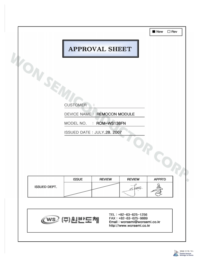
APPROVAL SHEET
advertisement

■ New APPROVAL SHEET CUSTOMER : DEVICE NAME : REMOCON MODULE MODEL NO. : ROMROM-WS138FN ISSUED DATE : JULY.28. .28. 2007 ISSUE REVIEW REVIEW APPR'D ISSUED DEPT. TEL : +82+82-6363-625625-1256 FAX : +82+82-6363-625625-9889 Email : wonsemi@wonsemi.co.kr http://www.wonsemi.co.kr http://www.wonsemi.co.kr □ Rev ROMROM-WS138FN IR Receiver Modules for Remote Control Systems Description The ROM-WT/WC/WS xxxxxxx (N)-X is a Bi-CMOS IC for use in infrared remote control system. It consist of automatic gain control amplifier,post amplifier, Oscillator, automatic gain control circuit, a band pass filter, a signal waveform detection circuit,automatic threshold control circuit, a waveform rectifier. Features • Supply Voltage Range: 2.7V ~ 6 V • TTL and CMOS compatibility • No external components Except PIN Diode • Available for Carrier Frequencies between 32.7kHz to 56.7kHz, ( Adjusted by zener-Diode Fusing, or using frequency selection PADs. (Refer to frequency selection table & bonding option.) ) • Internal filter for PCM frequency • Open collector output (built-in Pull-up resistor 40 ㏀ ) • Output active low • Enhanced Immunity against all kinds of disturbance light and power noise • No occurrence of disturbance pulses at output pin within nominal conditions. • Short settling time after power On ( below 1msec) Ordering Info.(carrier frequencies) Applications • TV, VCR, AUDIO • Home Appliances • Remote Control Equipment Type ROM-WT/WC/WSX32XX(N)-X ROM-WT/WC/WSX36XX(N)-X ROM-WT/WC/WSX38XX(N)-X ROM-WT/WC/WSX40XX(N)-X ROM-WT/WC/WSX56XX(N)-X Carrier Frequency 32.7 ㎑ 36.7 ㎑ 37.9 ㎑ 40.0 ㎑ 56.7 ㎑ Suitable Data Format NEC, RC5, RC6, Toshiba Micon Code, Sharp Code, Grundig Code Sony 12bit, Sony 15bit, Matsushita code, Mitsubishi Code, Zenith Code, JVC code Block Diagram VCC BGR IN 40Kohm Input Oscillator AGC AGC Control Post Amp. BPF Waveform Detector & ATC OUT Fc set Trimming Freq. selection 2/9 Waveform Rectifier GND http://www.wonsemi.co.kr http://www.wonsemi.co.kr ROMROM-WS138FN Application Guide Application for power supply ripple suppression 200Ω A further influence to the IR receiver modules may come from a Power supply VCC supply voltage which is not stable. Such a disturbed supply voltage 47uF can caused by switching power supply. which is not filtered well or by other components in the circuit which produced spikes on the supply line. This disturbed supply will reduce the sensitivity of receiver modules. This application circuit will filter the disturbed supply voltage. Absolute Maximum Ratings (Ta = 25℃) Parameter Symbol Min. Max. Unit Supply Voltage VCC 0 6.5 V Supply Current ICC 0 3 mA Output Voltage Vout 0 6.5 V Output Current Iout 0 2.5 mA Operating Temperature Tamb -25 85 ℃ Storage Temperature Tstg -30 85 ℃ Soldering Temperature Tsd 260℃±5℃, Max 5 sec ℃ ElectroElectro-optical Characteristics Parameter`` Supply Voltage (Ta = 25℃) Symbol Unit 2.7 - 6.0 V 0.8 1.2 1.5 3 0.5 0.9 1.2 5 -3 fo +3 3 -5 fo +5 - 940 - No input signal 5 VCC ICC B.P.F Center Frequency fO Peak Wave Length λP High Level Output Voltage VOH Fig.1 Low Level Output Voltage VOL Fig.1 High Level Output Pulse Width TWH Fig.1 Low Level Output Pulse Width TWL Fig.1 tPause Fig. 9 Arrival Distance Max Vcc Supply Current Minimum Data Pause Time between the data commands.(tPause) Typ Conditions L Output Form Fig. 1,2,3 Min 5 Vcc-0.5 - - 3 Vcc-0.5 - - 5 - 0.2 0.4 0.2 0.4 3 5 450 600 750 3 450 600 750 5 450 600 750 3 450 600 750 23 ㎃ % ㎚ V V ㎲ ㎲ ms ±0˚ - 25 - ±30˚ - 23 - ±45˚ - 20 - m Active Low ** Arrival Distance Effected by Environment 3/9 http://www.wonsemi.co.kr http://www.wonsemi.co.kr ROMROM-WS138FN Measurement Conditions [ Fig.1 ] f=37.9KHz, burst with 22 pulses 600 ㎲ 600 ㎲ Input Output pulse [ Fig.2 ] Transmitter 10㏀ VCC PD S/Transmitter 10㎌ VOUT 10㏀ GND 30㎝ ※ The specifications shall be satisfied under the following conditions. The standard transmitter shall be specified of the burst wave form adjusted to VOUT 200mVp-p upon Po measuring circuit Standard Transmitter [ Fig.3 ] Test condition of arrival distance Vout osc Transmitter GND Vcc : Indicates horizontal and vertical directions [ Measurement condition for arrival distance ] ☞ Ambient light source : Detecting surface illumination shall be irradiate 200±50Lux under ordinary white fluorescence lamp without high frequency lighting 4/9 http://www.wonsemi.co.kr http://www.wonsemi.co.kr ROMROM-WS138FN Electrical/Optical Characteristics [ Fig.5 ] Relative Spectral Sensitivity vs.Wavelength Supply Current(mA) S(λ)rel-Relative Spectral Sensitivity [ Fig.4 ] Supply Current vs. Voltage λ-Wavelength(nm) Supply Voltage(V) [ Fig.6 ] Output Pulse Width vs. Distance [ Fig.8 ] BPF Fc Curve [ Fig.7 ] Directivity (Horizontal/Vertical) ESD Test Results Relafive Amplitude Parameter Conditions Specification Results Machine Model C=200㎊, R=0Ω Min ±200V >±200V Human Body Model C=100㎊, R=1.5㏀ Min ±2000V >±2000V Charged Device Model R=100㏁, 1Ω Min ±800V >±800V Relafive Frequency 5/9 http://www.wonsemi.co.kr http://www.wonsemi.co.kr ROMROM-WS138FN Suitable Data Format The circuit of the ROM-WT/WC/WS XXXXX(N)-X series is designed in that way that unexpected output pulses due to noise or disturbance signals are avoided. A band pass filter, an integrator stage and an automatic gain control are used to suppress such disturbances. The distinguishing mark between data signal (not suppressed) and disturbance signal (suppressed) are carrier frequency, burst length and Signal Gap Time (see diagram below). The data signal should full-fill the following condition : Carrier frequency should be close to center frequency of the band-pass. Burst length should be 300us/burst or longer. After each burst a gap time of at least 300us is necessary. The data format should not make a continuous signal transmission. There must be a Signal Gap Time (longer than 23 ms) at least each 100 ms, or each data command. Some examples for suitable data format are : NEC Code, RC5, Toshiba Code, Matsushita Code. Mitsubishi Code. Sony Code. [ Fig. 9 ] Data Signal diagram Data Word enlarge t Burst t Pause Carrier Frequency : fo t Gap (Output pulse) ※ t Gap : Signal gap time between two burst in pulses of carrier. ※ t pause : Data pause between two data words. ※ t Burst : Length of a burst in pulses of the carrier frequency. Disturbance Suppression When a disturbance signal is applied to the ROM-WT/WC/WS XXXXX(N)-X series. it can still receive the data signal. However the sensitivity is reduced to that level that no unexpected pulses will occurrence. Some examples for such disturbance signals which are suppressed by the ROM-WT/WC/WS XXXXX(N)-X series are : Signals from fluorescent lamps with electronic ballast with high or low modulation. Continuous signal at 38 kHz or at any other frequency, DC light (from tungsten bulb or sunlight) 6/9 http://www.wonsemi.co.kr http://www.wonsemi.co.kr ROMROM-WS138FN ◆ External Dimension (Unit : mm) optical center 1 1 3 2 NOTE: 1. PIN CONFIG. 1 GND 2 Vout 3 Vcc 2. G.T ±0.3 (UNIT:mm) 7/9 http://www.wonsemi.co.kr http://www.wonsemi.co.kr ROMROM-WS138FN *** Packing unit for Remote control module*** 4.0 12.0 1.55 1.75 1) ROLL = 1000 pcs 12.00 ==== ==== Label #1 2) INNER BOX #1 = 14000pcs <Inner Box # 1> Outer Box #1 with Opto-Sensor Logo(365*360*270) (unit : mm) 4) Input 2 outer boxes into Box #2 == 28000pcs <Outer Box # 2> 8/9 Outer Box #2 with Opto-Sensor Logo (385*750*300) (unit : mm) http://www.wonsemi.co.kr http://www.wonsemi.co.kr ROMROM-WS138FN ** REEL 16.4 12 FRONT VIEW 9/9 http://www.wonsemi.co.kr http://www.wonsemi.co.kr


![[1] For the Multistage amplifier shown in Fig.1, RL = 250 Ω, RSig = 3](http://s2.studylib.net/store/data/018111916_1-f6a12ba465c3ae339f41af78ec6e65c7-300x300.png)