AVR317: Using the Master SPI Mode of the
USART module
8-bit
Microcontrollers
Features
•
•
•
•
Enables Two SPI buses in one device
Hardware buffered SPI communication
Polled communication example
Interrupt-controlled communication example
Application Note
Introduction
For the majority of applications, one Serial Peripheral Interface (SPI) module is
enough. However, some applications might need more than one SPI module. This
can be achieved using the Master SPI Mode of the devices with this feature such
as Atmega48.
The Synchronous Mode of the USART already has an external clock line to
synchronize the communication, but the start, stop and parity bits used in USART
communication are incompatible with SPI communication standards. In Master SPI
Mode, these extra bits are stripped off so that only the data bits are used. This
mode is therefore fully compatible with SPI communication standard, and it is
possible to use the USART as a SPI master.
The Master SPI Mode uses the same module as ordinary USART communication,
and therefore use the receive and transmit buffers. This makes hardware-buffered
SPI communication possible, which is not available in the standard SPI module.
This application note describes the steps necessary to setup and use the USART
in Master SPI Mode. It also provides code examples for both polled and interrupt
controlled communication. Detailed descriptions for the USART and SPI modules
and SPI communication in general are outside the scope of this document. The
reader should see the datasheets for this information.
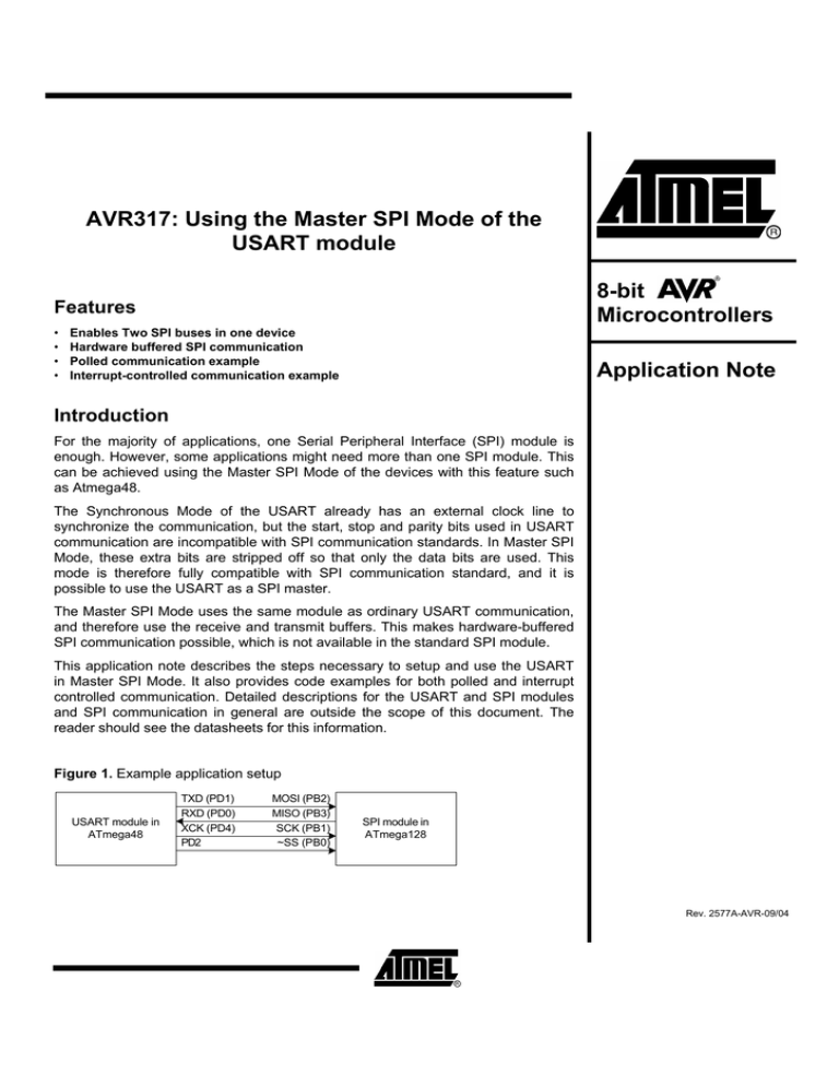
Figure 1. Example application setup
USART module in
ATmega48
TXD (PD1)
RXD (PD0)
XCK (PD4)
PD2
MOSI (PB2)
MISO (PB3)
SCK (PB1)
~SS (PB0)
SPI module in
ATmega128
Rev. 2577A-AVR-09/04
Theory of Operation
As described in the introduction, the ATmega48 USART has an extra mode called
Master SPI Mode (MSPIM). In this mode, the start, stop and parity bits are stripped
off from the communication frame, leaving only the data bits. Just as in Synchronous
Mode, the MSPIM use an external clock line (XCK) to synchronize master and slave.
Overview
Even if the USART supports 5 to 9 data bits and both master and slave operation,
enabling MSPIM automatically sets the USART in master mode with 8 data bits.
MSPIM uses the RXD, TXD and XCK lines, like the USART in Synchronous Mode.
These lines should be connected as shown in Figure 1. The USART Baud Rate
Register (UBRR) also has equal functionality in MSPIM and Synchronous Mode. This
means that the formulas for the UBRR value and resulting communication speed (bits
per second) are the same, as in Equation 1 below.
Equation 1. Communication speed calculation
bps =
SPI Compatibility
f OSC
f
⇔ UBRR = OSC − 1
2 ⋅ (UBRR + 1)
2 ⋅ bps
As a SPI Master, MSPIM is fully compatible with the SPI module. All four SPI modes
are available using the clock polarity and phase settings of the USART. The data bit
order can also be set to either LSB first or MSB first. The control bits are functionally
equivalent to the native SPI module.
All communication speeds available using the SPI prescaler can be generated with
the USART. UBRR is used instead of a prescaler; hence finer control of the
communication speed is possible.
The MSPIM is initialized in the same way as ordinary USART operation, except that
the USART Mode Select bits (UMSELn1:0) must be set to one to select MSPIM. The
XCK I/O pin must be configured manually as an output to enable master clock
generation.
Setup
To ensure that the XCK line is initialized correctly according to the SPI mode settings,
it is important that the UBRR is set to zero at the time the transmitter is enabled. After
enabling the transmitter, the correct value can be set.
Note that enabling the receiver is optional. It is ok to use the MSPIM as a SPI
transmitter only. Incoming data bits will be ignored and the RXD pin functionality will
not be overridden by the USART.
Byte transfer
When transferring bytes using the MSPIM, the three status flags have the same
functionality as in standard USART operation:
• The Receive Complete (RXC) flag is set when a byte has been received.
• The Transmit Complete (TXC) flag is set when a byte has been transmitted and
there are no more bytes waiting to be transmitted in the UDR buffer.
• The USART Data Register Empty (UDRE) flag is set when the UDR buffer is
empty, i.e. the UDR is ready for the next byte to be transmitted.
The closest equivalent to the SPI flag in the native SPI module is the TXC flag.
However, having the transmit buffers in the USART, there is no need to wait for the
TXC flag. A new byte can be written to UDR as soon as the UDRE flag is set. The
transmit buffers can therefore be used to achieve continuous transmission without
any delay between the bytes. This is not possible with the native SPI module.
2
AVR317
2577A-AVR-09/04
AVR317
When using the receiver, wait for the RXC flag and then read the received byte from
UDR. Note that it is the master device’s responsibility to give the slave device time to
prepare its next byte before starting a new transfer.
Implementation
The code examples that come with this application note show how to setup and use
the USART in MSPIM. There are two separate examples included, both written for
ATmega48. The first example uses software polling to check the USART flags. The
second example uses a circular buffer and interrupt-controlled communication.
The examples are designed for the STK500 Starter Kit with switches connected to
PORTB and LEDs connected to PORTC. The complete setup is shown in Figure 1
below.
Figure 2. Hardware setup
STK500 Switches
PORTB
SPI Master
(ATmega48)
TXD (PD1)
RXD (PD0)
XCK (PD4)
PD2
MOSI (PB2)
MISO (PB3)
SCK (PB1)
~SS (PB0)
SPI Slave
(ATmega128)
PORTC
STK500 LEDs
To be able to run the examples, a simple SPI slave is needed. This application note
therefore includes a small SPI slave application. The example is written for
ATmega128, but could easily be ported to any AVR with SPI. The SPI slave only
receives a byte, increments it and then transmits it when the connected master starts
the next SPI transfer. The detailed description of the SPI slave is outside the scope of
this document. Please refer to the datasheet of any AVR with SPI for details.
Polled version
The first example is very simple. It waits for the switches to be pressed or released,
transmits the value and puts the received value on the LEDs.
Note:
Main program flow
STK500 outputs logic low when switches are pressed, and the LEDs light up when
logic low is applied. Therefore the switch state is inverted before transmitting the
value, and the received value is inverted before being output to the LEDs. This is
done because it is more intuitive to let logic high represent switches pressed and
LEDs on.
The main program first initializes the USART in MSPIM. Then the SS line of the slave
is toggled once, to synchronize its SPI module. Finally the program enters an infinite
loop, transmitting switch states and outputting received values to the LEDs. The
flowchart is shown in Figure 3 below.
3
2577A-AVR-09/04
Figure 3. Polled version - Main program flow
START
(polled version)
Initialize UART in Master SPI
Mode
Toggle SS line once to
synchronize slave
Setup I/O for STK500 LEDs
and switches
No
Switch state
changed?
Yes
Queue switch state, its
inverse and a 0x00 byte
Set LED state to the third
received byte
USART initialization
The USART initialization subroutine performs the necessary operations to configure
the USART in Master SPI Mode. The flowchart is shown in Figure 4 below.
Figure 4. Polled version - USART initialization
Init USART
(polled version)
Set baud Rate Register to 0
Set XCK line to output mode
Select Master SPI Mode
(UMSELn1:0 = 11)
Set UCPOLn and UCPHAn to
required SPI mode
Enable Transmitter and
Receiver
Set Baud Rate Register to
required value
Return
4
AVR317
2577A-AVR-09/04
AVR317
Byte transfer
The transfer subroutine takes care of the byte transfer on the bus. It is named transfer
because SPI communication always transfers data. Separate transmission and
reception is not possible. The subroutine starts a transfer, waits for it to complete and
then returns the received value. The flowchart is shown in Figure 5 below.
Figure 5. Polled version - Byte transfer
SPI Transfer
(polled version)
No
UDR Empty?
Yes
Copy value to UDR
No
Transmit
Complete?
Yes
Return value from
UDR
Interrupt Controlled
version
The second example is a bit more complex than the first. It uses interrupt handlers for
the RXC and UDRE flags. The interrupt handlers communicate with the main program
through two circular buffers. One buffer is used for queuing data to be transmitted,
and one is used for queuing received data. This means that the communication driver
runs in the background, and the main program just have to fill the transmit buffer and
read from the receive buffer. The buffer structure is shown in Figure 6 below.
Figure 6. Circular TX and RX buffers
UDR Empty
Interrupt Handler
Queue value
Transmit buffer
tail
index
head
index
Receive Complete
Interrupt Handler
Fetch value
Receive buffer
tail
index
head
index
5
2577A-AVR-09/04
Note:
Main program flow
Since SPI communication combines transmission and reception in one operation,
every byte put in the TX buffer results in a byte being received and put in the RX
buffer. This also means that no byte will be put in the RX buffer without a byte being
put in the TX buffer first.
The main program first initializes the USART in MSPIM with interrupts enabled. Then
the SS line to the slave is toggled once, to synchronize its SPI module. Finally the
program enters the infinite loop. The flowchart is shown in Figure 7 below.
To demonstrate the buffer mechanism, three bytes are queued for transmission when
the switch state changes. The background driver performs the three transfers and
puts the three received bytes in the receive buffer. The last of the three bytes are
output on the LEDs. Using the example slave application that comes with this
application note, the third byte received is equal to the second one transmitted,
incremented once.
The three values transmitted are the switch state, its inverse and finally a zero byte.
Figure 7. Interrupt version - Main program flow
START
(interrupt version)
Initialize UART in Master SPI
Mode
Toggle SS line once to
synchronize slave
Setup I/O for STK500 LEDs
and switches
Enable global interrupts
No
Switch state
changed?
Yes
Queue switch state, its
inverse and a 0x00 byte
Set LED state to the third
received byte
USART initialization
6
The USART initialization subroutine for the interrupt-controlled version is almost
identical to the polled version. The only exception is that the RXC interrupt is enabled.
The UDRE interrupt, however, is not enabled in this subroutine. It is enabled by the
queuing subroutine when there are bytes to transmit in the TX buffer. The flowchart is
shown in Figure 8 below.
AVR317
2577A-AVR-09/04
AVR317
Figure 8. Interrupt version - USART initialization
Init USART
(interrupt version)
Set baud Rate Register to 0
Set XCK line to output mode
Select Master SPI Mode
(UMSELn1:0 = 11)
Set UCPOLn and UCPHAn to
required SPI mode
Enable Transmitter, Receiver
and RX Complete Interrupt
Set Baud Rate Register to
required value
Return
Queue value
The main program calls this subroutine when it wants to transmit a byte. It puts the
byte in the TX buffer and enables the UDRE interrupt. The interrupt handler will
disable the UDRE interrupt when the TX buffer is empty. The flowchart is shown in
Figure 9 below.
Note:
The example application does not perform any buffer overflow control, but the
designer could easily implement that in actual designs if necessary.
Figure 9. Interrupt version - Queue value
Queue value
(interrupt version)
Put value at TX buffer head
position
Advance TX buffer head
index and wrap to 0 if
necessary
Enable UDR Empty Interrupt
Return
Fetch value
The main program calls this subroutine when it wants to read a byte that has been
received. It fetches the oldest byte from the RX buffer and returns it. If the buffer is
empty, it waits for a byte to be received. The flowchart is shown in Figure 10 below.
7
2577A-AVR-09/04
Figure 10. Interrupt version - Fetch value
Fetch value
(interrupt version)
Yes
Receive buffer
empty?
No
Get value from RX buffer tail
position
Advance RX buffer tail index
and wrap to 0 if necessary
Return value
USART Data Register Empty
Interrupt Handler
This interrupt handler is called when the USART hardware removes a byte from the
UDR and starts transmitting it. The UDR then has room for the next byte. The
interrupt handler moves the oldest byte from the TX buffer to the UDR. If the buffer is
empty the UDRE interrupt is disabled. The flowchart is shown in Figure 11 below.
Figure 11. Interrupt version - UDRE Interrupt Handler
UDR Empty
Interrupt Handler
Transmit value from TX buffer
tail position
Advance TX buffer tail index
and wrap to 0 if necessary
TX buffer
empty?
Yes
Disable UDR Empty Interrupt
No
Return
Receive Complete Interrupt
Handler
8
This interrupt handler is called when the USART has received a byte. In MSPIM this
happens automatically when a byte is transmitted. The interrupt handler puts the
received value into the receive buffer, without any overflow control. The flowchart is
shown in Figure 12 below.
AVR317
2577A-AVR-09/04
AVR317
Figure 12. Interrupt version - RXC Interrupt Handler
Receive Complete
Interrupt Handler
Put received value at RX
buffer head position
Advance RX buffer head
index and wrap to 0 if
necessary
Return
Literature References
• ATmega48/88/168 Datasheet (Rev. C)
9
2577A-AVR-09/04
Disclaimer
Atmel Corporation
2325 Orchard Parkway
San Jose, CA 95131, USA
Tel: 1(408) 441-0311
Fax: 1(408) 487-2600
Regional Headquarters
Europe
Atmel Sarl
Route des Arsenaux 41
Case Postale 80
CH-1705 Fribourg
Switzerland
Tel: (41) 26-426-5555
Fax: (41) 26-426-5500
Asia
Room 1219
Chinachem Golden Plaza
77 Mody Road Tsimshatsui
East Kowloon
Hong Kong
Tel: (852) 2721-9778
Fax: (852) 2722-1369
Japan
9F, Tonetsu Shinkawa Bldg.
1-24-8 Shinkawa
Chuo-ku, Tokyo 104-0033
Japan
Tel: (81) 3-3523-3551
Fax: (81) 3-3523-7581
Atmel Operations
Memory
2325 Orchard Parkway
San Jose, CA 95131, USA
Tel: 1(408) 441-0311
Fax: 1(408) 436-4314
Microcontrollers
2325 Orchard Parkway
San Jose, CA 95131, USA
Tel: 1(408) 441-0311
Fax: 1(408) 436-4314
La Chantrerie
BP 70602
44306 Nantes Cedex 3, France
Tel: (33) 2-40-18-18-18
Fax: (33) 2-40-18-19-60
ASIC/ASSP/Smart Cards
Zone Industrielle
13106 Rousset Cedex, France
Tel: (33) 4-42-53-60-00
Fax: (33) 4-42-53-60-01
RF/Automotive
Theresienstrasse 2
Postfach 3535
74025 Heilbronn, Germany
Tel: (49) 71-31-67-0
Fax: (49) 71-31-67-2340
1150 East Cheyenne Mtn. Blvd.
Colorado Springs, CO 80906, USA
Tel: 1(719) 576-3300
Fax: 1(719) 540-1759
Biometrics/Imaging/Hi-Rel MPU/
High Speed Converters/RF Datacom
Avenue de Rochepleine
BP 123
38521 Saint-Egreve Cedex, France
Tel: (33) 4-76-58-30-00
Fax: (33) 4-76-58-34-80
1150 East Cheyenne Mtn. Blvd.
Colorado Springs, CO 80906, USA
Tel: 1(719) 576-3300
Fax: 1(719) 540-1759
Scottish Enterprise Technology Park
Maxwell Building
East Kilbride G75 0QR, Scotland
Tel: (44) 1355-803-000
Fax: (44) 1355-242-743
Literature Requests
www.atmel.com/literature
Disclaimer: The information in this document is provided in connection with Atmel products. No license, express or implied, by estoppel or
otherwise, to any intellectual property right is granted by this document or in connection with the sale of Atmel products. EXCEPT AS SET
FORTH IN ATMEL’S TERMS AND CONDITIONS OF SALE LOCATED ON ATMEL’S WEB SITE, ATMEL ASSUMES NO LIABILITY
WHATSOEVER AND DISCLAIMS ANY EXPRESS, IMPLIED OR STATUTORY WARRANTY RELATING TO ITS PRODUCTS INCLUDING,
BUT NOT LIMITED TO, THE IMPLIED WARRANTY OF MERCHANTABILITY, FITNESS FOR A PARTICULAR PURPOSE, OR NONINFRINGEMENT. IN NO EVENT SHALL ATMEL BE LIABLE FOR ANY DIRECT, INDIRECT, CONSEQUENTIAL, PUNITIVE, SPECIAL OR
INCIDENTAL DAMAGES (INCLUDING, WITHOUT LIMITATION, DAMAGES FOR LOSS OF PROFITS, BUSINESS INTERRUPTION, OR
LOSS OF INFORMATION) ARISING OUT OF THE USE OR INABILITY TO USE THIS DOCUMENT, EVEN IF ATMEL HAS BEEN ADVISED
OF THE POSSIBILITY OF SUCH DAMAGES. Atmel makes no representations or warranties with respect to the accuracy or completeness of
the contents of this document and reserves the right to make changes to specifications and product descriptions at any time without notice.
Atmel does not make any commitment to update the information contained herein. Atmel’s products are not intended, authorized, or warranted
for use as components in applications intended to support or sustain life.
© Atmel Corporation 2004. All rights reserved. Atmel®, logo and combinations thereof, AVR®, and AVR Studio® are registered trademarks,
and Everywhere You Are™ are the trademarks of Atmel Corporation or its subsidiaries. Other terms and product names may be trademarks of
others.
2577A-AVR-09/04
