USCi Cascode in High Voltage Phase Shift Full Bridge
advertisement
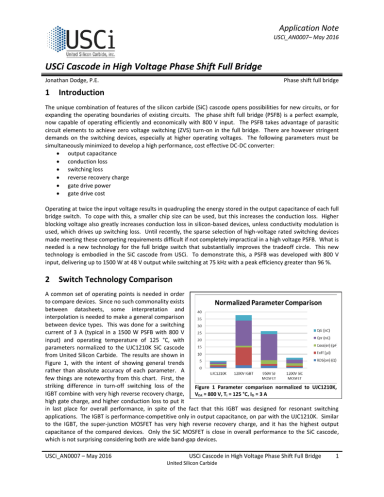
Application Note USCi_AN0007– May 2016 USCi Cascode in High Voltage Phase Shift Full Bridge Jonathan Dodge, P.E. 1 Phase shift full bridge Introduction The unique combination of features of the silicon carbide (SiC) cascode opens possibilities for new circuits, or for expanding the operating boundaries of existing circuits. The phase shift full bridge (PSFB) is a perfect example, now capable of operating efficiently and economically with 800 V input. The PSFB takes advantage of parasitic circuit elements to achieve zero voltage switching (ZVS) turn-on in the full bridge. There are however stringent demands on the switching devices, especially at higher operating voltages. The following parameters must be simultaneously minimized to develop a high performance, cost effective DC-DC converter: output capacitance conduction loss switching loss reverse recovery charge gate drive power gate drive cost Operating at twice the input voltage results in quadrupling the energy stored in the output capacitance of each full bridge switch. To cope with this, a smaller chip size can be used, but this increases the conduction loss. Higher blocking voltage also greatly increases conduction loss in silicon-based devices, unless conductivity modulation is used, which drives up switching loss. Until recently, the sparse selection of high-voltage rated switching devices made meeting these competing requirements difficult if not completely impractical in a high voltage PSFB. What is needed is a new technology for the full bridge switch that substantially improves the tradeoff circle. This new technology is embodied in the SiC cascode from USCi. To demonstrate this, a PSFB was developed with 800 V input, delivering up to 1500 W at 48 V output while switching at 75 kHz with a peak efficiency greater than 96 %. 2 Switch Technology Comparison A common set of operating points is needed in order to compare devices. Since no such commonality exists between datasheets, some interpretation and interpolation is needed to make a general comparison between device types. This was done for a switching current of 3 A (typical in a 1500 W PSFB with 800 V input) and operating temperature of 125 °C, with parameters normalized to the UJC1210K SiC cascode from United Silicon Carbide. The results are shown in Figure 1, with the intent of showing general trends rather than absolute accuracy of each parameter. A few things are noteworthy from this chart. First, the striking difference in turn-off switching loss of the Figure 1 Parameter comparison normalized to UJC1210K, IGBT combine with very high reverse recovery charge, VDS = 800 V, Tj = 125 °C, ID = 3 A high gate charge, and higher conduction loss to put it in last place for overall performance, in spite of the fact that this IGBT was designed for resonant switching applications. The IGBT is performance-competitive only in output capacitance, on par with the UJC1210K. Similar to the IGBT, the super-junction MOSFET has very high reverse recovery charge, and it has the highest output capacitance of the compared devices. Only the SiC MOSFET is close in overall performance to the SiC cascode, which is not surprising considering both are wide band-gap devices. USCi_AN0007 – May 2016 USCi Cascode in High Voltage Phase Shift Full Bridge United Silicon Carbide 1 Phase shift full bridge 3 www.unitedsic.com High Voltage PSFB Design Considerations The maximum resonant inductance is limited by the loss of duty cycle Δd from primary to secondary side of the transformer and by the switching frequency. 𝑁𝑡𝑢𝑟𝑛𝑠 ∙ 𝑉𝑖𝑛 𝐿𝑟𝑒𝑠(max) = ∆𝑑 ∙ 4 ∙ 𝐼𝑜𝑢𝑡 ∙ 𝑓𝑠𝑤 Notice that the maximum resonant inductance is determined by operating conditions rather than switching device characteristics. Keeping the output power and voltage fixed, doubling the input voltage requires doubling the transformer turns ratio Nturns, hence the maximum resonant inductance value increases fourfold. The minimum resonant inductance needed to support ZVS turn-on can be calculated by equating the energy stored in the resonant inductance and capacitance. The output capacitances of the two switches in each leg of the fullbridge are effectively in parallel during switching transitions, so twice the energy-related output capacitance Coss(er) from the device datasheet is added to the estimated transformer capacitance to calculate the resonant capacitive energy stored, which is Cres. The resonant inductance Lres is the combination of the transformer leakage and magnetizing inductances plus the shim inductance (if used). The primary-side current Ipri is the current through the resonant inductance at the switching event in the passive-to-active (PtoA) leg. 2 𝑉𝑖𝑛 𝐿𝑟𝑒𝑠(𝑚𝑖𝑛) = 𝐶𝑟𝑒𝑠 ∙ ( ) 𝐼𝑝𝑟𝑖 The minimum resonant inductance is determined by operating conditions and largely by switching device output capacitance. Again keeping the output power and voltage fixed, doubling the input voltage increases the minimum resonant inductance value by sixteen times. Obviously the maximum resonant inductance value must exceed the minimum value. To this end, decreasing the switching frequency can make the power converter commercially unattractive. Increasing the duty cycle loss limits the input and output operating voltage ranges. The only “knob to turn” to make a high voltage PSFB design feasible is a reduced output capacitance, which is why this parameter is so critical. The USCi cascode has bestin-class RDS(on) · area product, resulting in the lowest RDS(on) · Coss tradeoff curve of any device type. The low duty cycle loss and higher switching frequency range can translate into the widest voltage ranges with commercially attractive passive component selection. Figure 2 Efficiency versus output power at various output voltages System-level costs are further reduced via low cost gate drive circuitry. While capable of up to ±20 V, the cascode is fully enhanced with 10 V and can be driven from a single power supply, especially with the noise immunity of a 4.5 V typical threshold voltage. The symmetric gate voltage range allows the use of low cost gate transformers for isolation without clamp zeners and transistors. The extremely low recovery charge and smooth recovery characteristic of the intrinsic anti-parallel diode make the cascode completely safe to use, even if ZVS condition is lost. Furthermore, the low forward voltage ensures high efficiency under all operating conditions, eliminating the need for a separate anti-parallel diode. The performance of the USCi UJC1210K cascode was demonstrated in a PSFB with 700 to 820 V input, capable of delivering 1500 W at 48 to 60 V, switching at 75 kHz. Some efficiency results are shown in Figure 2 at 800 V input and various output voltages. The peak efficiency exceeds 96 % with the nominal 48 V output, opening many possibilities for new applications with higher operating voltage and system-level efficiency improvements. For example, a high voltage PSFB paired with an active rectifier fed by 480 VAC could greatly improve the cost and efficiency of power distribution in data centers. 2 USCi Cascode in High Voltage Phase Shift Full Bridge United Silicon Carbide USCi_AN0007 – May 2016

