Application Note | Case Study | Technology Feature | White Paper
High speed low light imaging:
escaping the shot noise limit
Noise is an important topic for
all machine vision applications,
especially if the requirements on
image quality and speed are high
and light levels are low. Changing
parameters usually leads to an
increase in noise. Bucking this trend,
a novel dual-linescan architecture
provides a way to preserve higher
signal-to-noise ratio.
Machine vision applications constantly present sensor and camera
designers with conflicting goals: higher resolution (to detect smaller
features), higher speed (for faster inspection), higher sensitivity (for
shorter exposures with less light), and lower noise (for better image
quality). Nowhere are these demands stronger than in linescan
applications, almost all of which have become high-speed low-light
challenges. Conventional linescan designs are now approaching
fundamental limits. In high-speed, low-light situations, photon
shot noise, which depends on the number of photons detected
rather than the electrons they generate, is becoming a limiter to
image quality.
Higher resolution. As mentioned, inspection applications demand
ever-greater resolution to detect smaller features with greater clarity.
To make use of existing, economical lenses, pixels must be smaller
to fit more of them into a given lens’s imaging circle. Smaller pixels
come at a price; they have less total area to collect photons, which
limits the signal they can collect.
Higher scan rates. The need for speed is clear in machine vision.
Faster inspection enables increased inspection system efficiency.
Sensor designers have worked hard to deliver steady progress in
pixel rates and amplifier bandwidth for greater speed. But higher
speed often means higher noise, so image sensor designers have
also worked hard to limit noise in their high-bandwidth amplifiers.
Progress has again been steady, but not enough to keep the noise
floor constant.
Less light. Higher scan rates reduce the time available to capture
photons. With less time to collect the light applications need either
higher light intensity or higher pixel sensitivity. Extremely intense light
sources bring their own challenges—they deliver more photons, but
they raise system cost, and not only can they damage the objects
being inspected, they can even pose safety hazards. With each
increase in speed, sensor designers have had to try to increase
sensitivity.
Higher sensitivity. In the quest to deliver more signal, merely
applying gain to amplify a weak signal is not the answer, since it
also amplifies noise. To improve SNR, imagers must derive more
signal from each photon while still controlling noise. Successive
generations of devices have shown significant improvements in
charge conversion efficiency (CCE) through better pixel designs
and advances in wafer foundry processes, but sensitivity has not
quite kept pace with speed increases. As a result, camera noise
floors have steadily increased over the last decade, and SNR,
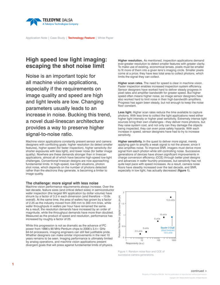
especially in low light, has actually decreased (figure 1).
The challenge: more signal with less noise
While this progression is not as dramatic as the advance of PC
power from 1996’s 90 MHz Pentium chips to 2006’s 3.4+ GHz
64-bit processors, imaging engineers can still feel justifiable pride.
Whether designers can make similar improvements in the next 10
years remains to be seen. Imaging performance is ultimately limited
by analog operations, and machine vision applications present
divergent goals that will press against fundamental limits of physics.
2
Random Noise Floor (digital counts pk-pk)
Machine vision performance requirements always increase. Over the
last decade, feature sizes (and critical defect sizes) in semiconductor
wafer inspection (the largest MV application by dollar volume) have
shrunk by a factor of 3.3 in each dimension (and therefore ~10.8x
overall). At the same time, the area of wafers has grown by a factor
of 2.25 as the industry moved from 200 mm to 300 mm lines, while
wafer throughputs in wafers per hour have remained the same.
As a result, the resolution demands have increased by an order of
magnitude, while the throughput demands have more than doubled.
Measured as the product of speed and resolution, performance has
increased by roughly a factor of 25.
13.5 uV/e
1.5
10 uV/e
1
5 uV/e
0.5
Spyder 3 GigE
(dual linescan)
13.5 uV/e
3 uV/e
2.5 uV/e
0
1
10
100
1000
Responsivity (a.u.)
Figure 1: Random noise floor and CCE of
successive camera generations.
1
continued >
Property of Teledyne DALSA. Not for publication or reproduction without permission.
Copyright © 2011 Teledyne DALSA Corporation. All Rights Reserved.
Application Note | Case Study | Technology Feature | White Paper
Lower noise. Noise is critical to any electronic system, and imagers
are subject to a variety of noise sources. Amplifier noise, as already
mentioned, requires sensor designers to expend significant effort in
optimization. Reset noise is caused by the act of resetting capacitors
on the sensor to a known level before they are used for the next
exposures. Reset noise can be removed by correlated double
sampling, either on-chip or off-chip. Sensors will also exhibit fixed
pattern noise from various sources. Fortunately, regardless of source,
if noise has a fixed pattern, it can be deterministically removed by
subtraction (or addition).
But there is no quick fix for photon shot noise, a statistical
phenomenon following a Poisson distribution resulting from the
random variation in the number of discrete electrons captured when
photons strike the photosensor. Photon shot noise is particularly
problematic in high-speed low-light imaging, since it depends not on
the signal voltage generated by the photons, but on the number of
photons themselves. Arising from the quantum nature of light, photon
shot noise cannot be separated from the signal itself. It is present
before any signal processing or output operations, even before the
act of detection. Increasing CCE to generate more voltage from each
electron will not improve the signal to shot noise ratio.
Furthermore, photon shot noise has a sub-linear relationship with
detected photons—it scales with the square root of the number
of photons detected (figure 2). Doubling the number of photons
only increases the shot noise by √2, and while this is good for
bright light, it is bad for low light, since reducing photons by 50%
(1/2) only reduces shot noise by ~30% (1–1/√2). As the available
light decreases, photon shot noise becomes a progressively more
dominant noise source. Despite advances in controlling any other
noise sources, eventually shot noise will limit sensor and camera
noise floors.
Dodging shot noise with dual linescan
If photon shot noise limits performance, then the goal of designers
will be to increase the number of photons collected. But with
constraints on the size of pixels, the light intensity, and the exposure
period, there are few options left for gathering more photons.
Increasing quantum efficiency (QE) to capture as many available
photons as possible is an obvious option, but boosting QE through
processes like backside thinning is tricky and expensive.
A dual linescan CCD offers another path to collecting more photons,
without requiring any semiconductor process development. Simply
put, the design takes two exposures and combines them, doubling
sensitivity with only a √2 increase in shot noise and thereby
delivering a greater signal to noise ratio.
Functionally similar to TDI (time delay and integration) arrays, the
design consists of two parallel arrays of photodiode pixels. Having
twice the pixel area allows it to capture twice the number of photons
compared to a single line with the same QE and CCE.
Each pixel is connected to a selectable delay gate that either
allows charges through or delays the charges by one scan line
(figure 3). As in all linescan devices, the line rate of the sensor must
be matched to the motion of the object being imaged. If the image
of the object scanned is moving from the top to the bottom of the
sensor, the top array receives signals one line prior to the bottom
array. It then stores the collected charge in a delay line before
combining it with the charge collected from the bottom array.
Thus, the sensor can effectively combine two exposures.
Signal electrons from the two arrays (one delayed, one not) are
combined on-chip into a single output. Since the charge is combined
before the output amplifier, there is no increase in amplifier noise.
Like conventional linescan but unlike TDI, dual linescan allows
exposure control. And its photodiode design is free of extra silicon
gates that can interfere with blue response.
Storage Well with Anti-blooming and Exposure Control
OS2
Storage Well with Anti-blooming and Exposure Control
Selectable One Line Delay
RelayReverse
Merge
N Photodiodes
Merge
Photon Shot Noise
RelayForward
N Photodiodes
OS1
(a.u.)
Detected Photons
Selectable One Line Delay
Merge
Merge
CCD Readout Shift Register
CCD Readout Shift Register
Figure 3: Structure of dual line scan sensor
Exposure
Figure 2: Detected photons and photon shot noise:
sub-linear relationship.
2
continued >
Property of Teledyne DALSA. Not for publication or reproduction without permission.
Copyright © 2011 Teledyne DALSA Corporation. All Rights Reserved.
The main disadvantage of this design is an increase in dark signal
from the doubled pixel area. But as mentioned earlier, most linescan
applications call for high speed and very short exposures. In
situations like these, the integration time is so short that the dark
signal is negligible.
At first glance, it appears that the CCD capacitance (and hence the
power dissipation) is twice that of a conventional linescan. However,
each of the two CCD readout registers only needs to handle half the
amount of signal charge, so the CCD capacitance is less than double
that of a conventional linescan.
Proof of the design’s high-speed low-light effectiveness can be found
in Spyder 3 GigE linescan camera. In addition to the patented dual
linescan architecture, the camera benefits from improved CCE so
that it delivers three times the responsivity of its predecessor. It also
delivers twice its predecessor’s line rates (figure 4).
Photon Shot Noise (digital counts pk-pk)
20
Conventional Designs
Spyder 3 GigE (dual line scan)
10
0
1
10
100
1000
Responsivity (a.u.)
Figure 4: Photon shot noise as a function of
responsivity
www.teledynedalsa.com
Americas
Boston, USA
+1 978-670-2000
sales.americas@teledynedalsa.com
Europe
Munich, Germany
+49 8142-46770
sales.europe@teledynedalsa.com
Asia Pacific
Tokyo, Japan
+81 3-5960-6353
sales.asia@teledynedalsa.com
Teledyne DALSA has its corporate offices in Waterloo, Canada
Teledyne DALSA reserves the right to make changes at any time without notice. Teledyne DALSA © 2011. 03-070-20022-01
Shanghai, China
+86 21-3368-0027
sales.asia@teledynedalsa.com


