GS9068 SD SDI Cable Driver
Key Features
Description
•
SMPTE 259M and SMPTE 344M compliant
•
Dual coaxial cable driving outputs
•
50Ω differential PECL input
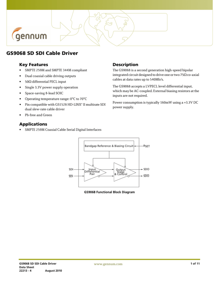
The GS9068 is a second generation high-speed bipolar
integrated circuit designed to drive one or two 75Ω co-axial
cables at data rates up to 540Mb/s.
•
Single 3.3V power supply operation
•
Space-saving 8-lead SOIC
•
Operating temperature range: 0°C to 70°C
•
Pin compatible with GS1528 HD-LINX® II multirate SDI
dual slew-rate cable driver
•
Pb-free and Green
The GS9068 accepts a LVPECL level differential input,
which may be AC-coupled. External biasing resistors at the
inputs are not required.
Power consumption is typically 160mW using a +3.3V DC
power supply.
Applications
•
SMPTE 259M Coaxial Cable Serial Digital Interfaces
SDI
SDI
Bandgap Reference & Biasing Circuit
RSET
Input
Differential
Pair
SDO
Output
Stage
& Control
SDO
GS9068 Functional Block Diagram
GS9068 SD SDI Cable Driver
Data Sheet
22213 - 4
August 2010
www.gennum.com
1 of 11
Contents
1. Pin Out...............................................................................................................................................................3
1.1 Pin Assignment ..................................................................................................................................3
1.2 Pin Descriptions ................................................................................................................................3
2. Electrical Characteristics ............................................................................................................................4
2.1 Absolute Maximum Ratings ..........................................................................................................4
2.2 DC Electrical Characteristics ........................................................................................................4
2.3 AC Electrical Characteristics ........................................................................................................5
3. Detailed Description.....................................................................................................................................6
3.1 Serial Digital Input ...........................................................................................................................6
3.2 Serial Digital Output ........................................................................................................................6
3.3 Output Return Loss Measurement ..............................................................................................7
3.4 Output Amplitude Adjustment ....................................................................................................7
4. Application Reference Design ..................................................................................................................9
4.1 PCB Layout ..........................................................................................................................................9
4.2 Typical Application Circuit ...........................................................................................................9
5. References........................................................................................................................................................9
6. Package and Ordering Information...................................................................................................... 10
6.1 Package Dimensions ..................................................................................................................... 10
6.2 Ordering Information ................................................................................................................... 10
7. Revision History.......................................................................................................................................... 10
GS9068 SD SDI Cable Driver
Data Sheet
22213 - 4
August 2010
2 of 11
1. Pin Out
1.1 Pin Assignment
SDI
1
SDI
2
VEE
3
RSET
4
GS9068
8-pin SOIC
(top view)
8
SDO
7
SDO
6
NC
5
VCC
Figure 1-1: Pin Assignment
1.2 Pin Descriptions
Pin
Number
Name
Type
1, 2
SDI, SDI
Input
Serial digital differential input.
3
VEE
Input
Power
Most negative power supply connection - connect to GND.
4
RSET
Input
External output amplitude control resistor.
5
VCC
Input
Power
Most positive power supply connection - connect to +3.3V.
6
NC
—
7, 8
SDO, SDO
Output
GS9068 SD SDI Cable Driver
Data Sheet
22213 - 4
August 2010
Description
No Connect.
Serial digital differential output.
3 of 11
2. Electrical Characteristics
2.1 Absolute Maximum Ratings
Table 2-1: Absolute Maximum Ratings
Parameter
Value
Supply Voltage
-0.5V to 3.6 VDC
Input ESD Voltage
500V
Storage Temperature Range
-50°C < Ts < 125°C
Input Voltage Range (any input)
-0.3 to (VCC +0.3)V
Operating Temperature Range
0°C to 70°C
Power Dissipation
300mW
Lead Temperature (soldering, 10
sec)
260°C
2.2 DC Electrical Characteristics
Table 2-2: DC Electrical Characteristics
Parameter
Symbol
Conditions
Min
Typical
Max
Units
Test
Level
Supply Voltage
VCC
3.1
3.3
3.5
V
3
Power
Consumption
PD
-
160
-
mW
5
Supply Current
Is
-
48
-
mA
1
Output Voltage
VOC
Common mode
-
VCC - ΔVSDO(SE)
-
mV
6
Input Voltage
VIC
Common mode
1.6 + ΔVSDI(DIFF)/2
-
VCC - ΔVSDI(DIFF)/2
mV
1
GS9068 SD SDI Cable Driver
Data Sheet
22213 - 4
August 2010
4 of 11
2.3 AC Electrical Characteristics
Table 2-3: AC Electrical Characteristics
Parameter
Symbol
Conditions
Min
Typical
Max
Units
Test
Level
Serial input data rate
DRSDI
—
—
—
540
Mb/s
1
Input Voltage Swing
ΔVSDI(DIFF)
Differential
300
—
2200
mVp-p
1
Output Voltage Swing
ΔVSDO(SE)
single-ended into a 75Ω
external load
750
800
850
mVp-p
1
RSET = 750Ω
Additive jitter
—
—
—
—
30
ps
1
Rise/Fall time
tr/tf
20% to 80%
400
—
800
ps
1
Δtr/Δtf
—
—
—
30
ps
1
Mismatch in rise/fall time
Duty cycle distortion
—
—
—
—
100
ps
1
Overshoot
—
—
—
—
8
%
1
ORL
—
15
—
—
dB
7
Output Return Loss
TEST LEVELS
1. Production test at room temperature and nominal supply voltage with guard
bands for supply and temperature ranges.
2. Production test at room temperature and nominal supply voltage with guard
bands for supply and temperature ranges using correlated test.
3. Production test at room temperature and nominal supply voltage.
4. QA sample test.
5. Calculated result based on Level 1, 2, or 3.
6. Not tested. Guaranteed by design simulations.
7. Not tested. Based on characterization of nominal parts.
8. Not tested. Based on existing design/characterization data of similar product.
9. Indirect test.
10.Wafer Probe.
GS9068 SD SDI Cable Driver
Data Sheet
22213 - 4
August 2010
5 of 11
3. Detailed Description
3.1 Serial Digital Input
SDI/SDI are high-impedance differential inputs. Several conditions must be observed
when interfacing to these inputs:
1. The differential input signal amplitude must be between 300 and 2000mVpp.
2. For DC-coupling to the device, the common mode voltage must be between
1.6+ΔVSDI(DIFF) and VCC-ΔVSDI(DIFF).
3. For input trace lengths longer than approximately 1cm, the inputs should be
terminated as shown in the Typical Application Circuit.
The GS9068 inputs are self-biased, allowing for simple AC-coupling to the device. For
serial digital video, a minimum capacitor value of 4.7μF should be used to allow
coupling of pathological test signals. A tantalum capacitor is recommended.
3.2 Serial Digital Output
The GS9068 outputs are current mode, and will drive 800mV into a 75Ω load. These
outputs are protected from accidental static damage with internal static protection diodes.
The SMPTE 259M standard requires that the output of a cable driver have a source
impedance of 75Ω and a return loss of at least 15dB between 5MHz and 540MHz. In order
for an SDI output circuit using the GS9068 to meet this specification, the output circuit
shown in the Typical Application Circuit is recommended.
The value of LCOMP will vary depending on the PCB layout, with a typical value of 5.6nH.
A 4.7μF capacitor is used for AC-coupling the output of the GS9068. This value is chosen
to ensure that pathological signals can be coupled without a significant DC component
occurring (see Section 4. Application Reference Design, for more details).
When measuring return loss at the GS9068 output, it is necessary to take the
measurement for both a logic high and a logic low output condition. This is because the
output protection diodes act as a varactor (voltage controlled capacitor) as shown in
Figure 3-1. Consequently, the output capacitance of the GS9068 is dependent on the
logic state of the output.
SDO
SDO
Figure 3-1: Static Protection Diodes
GS9068 SD SDI Cable Driver
Data Sheet
22213 - 4
August 2010
6 of 11
3.3 Output Return Loss Measurement
To perform a practical return loss measurement, it is necessary to force the GS9068
output to a DC high or low condition. The actual return loss will be based on the outputs
being static at VCC or VCC-1.6V. Under normal operating conditions, the outputs of the
GS9068 swing between VCC-0.4V and VCC-1.2V, hence the measured value of return
loss will not represent the actual operating return loss.
A simple method of calculating the values of actual operating return loss is to interpolate
the two return loss measurements. In this method, the values of return loss are estimated
at VCC-0.4V and VCC-1.2V based on the measurements at VCC and VCC-1.6V.
The two values of return loss (high and low) will typically differ by several decibels. If
the measured return loss is RH for logic high and RL for logic low, then the two values can
be interpolated as follows:
RIH = RH- (RH-RL)/4, and
RIL = RL+(RH-RL)/4
Where RIH is the interpolated logic high value and RIL is the interpolated logic low value.
For example: if RH = -18dB and RL = -14dB; the interpolated values are RIH = -17dB and
RIL = -15dB.
3.4 Output Amplitude Adjustment
The output amplitude of the GS9068 can be adjusted by changing the value of the RSET
resistor as shown in Figure 3-2 and Table 3-1 below. For an 800mVp-p output with a
nominal ±7% tolerance, a value of 750Ω is required. A ±1% SMT resistor should be used.
Output Swing (mV)
1100
1000
900
800
700
600
500
600
700
800
900
1000
RSET (W)
Figure 3-2: Output Amplitude Adjustment
The RSET resistor is part of the high-speed output circuit of the GS9068. The resistor
should be placed as close as possible to the RSET pin. In addition, the PCB capacitance
should be minimized at this node by removing the PCB ground plane beneath the RSET
resistor and the RSET pin.
GS9068 SD SDI Cable Driver
Data Sheet
22213 - 4
August 2010
7 of 11
Table 3-1: RSET vs. VOD
RSET (Ω)
Output Swing
995
608mV
824
734mV
750
800mV
600
884mV
573
1040mV
NOTE: For reliable operation of the GS9068 over the full temperature range, do not use
an RSET value below 573Ω.
GS9068 SD SDI Cable Driver
Data Sheet
22213 - 4
August 2010
8 of 11
4. Application Reference Design
4.1 PCB Layout
An FR-4 dielectric can be used, however, controlled-impedance transmission lines are required
for PCB traces longer than approximately 1cm. Note the following PCB artwork features used to
optimize performance:
•
The PCB groundplane is removed under the GS9068 output components to minimize
parasitic capacitance
•
The PCB ground plane is removed under the GS9068 RSET pin and resistor to minimize
parasitic capacitance
•
Input and output BNC connectors are surface-mounted in-line to eliminate a
transmission line stub caused by a BNC mounting via high-speed traces, which are
curved to minimize impedance variations due to change of PCB trace width
4.2 Typical Application Circuit
5.6n*
BNC
4µ7
75
49.9
1
2
3
10n
49.9
Differential
Data Input
4µ7
4
SDI
SDI
VEE
RSET
GS9068
SDO
SDO
NC
VCC
75
8
7
6
VCC
10n
75
5
75
BNC
5.6n*
4µ7
VCC
4µ7
750
VCC
10n
*typical value, varies with layout
NOTE: All resistors in Ohms, capacitors in Farads,
and inductors in Henrys, unless otherwise noted.
Figure 4-1: Typical Application Circuit
5. References
Compliant with SMPTE 259M and SMPTE 344M.
GS9068 SD SDI Cable Driver
Data Sheet
22213 - 4
August 2010
9 of 11
6. Package and Ordering Information
D
X
E
0.010
Gauge Plane
Seating Plane
q2
Pin 1
ID Mark
e
B
L
DETAIL “A”
Max.
A
0.054
A1
B
0.004
0.068
0.0098
0.019
D
E
0.196
0.157
0.244
0.229
0.050 BSC
C
L
C
q1
A1
Min.
H
e
DETAIL “A”
0.015 ±0.004 x 45°
A
SYMBOL
6.1 Package Dimensions
8 SOIC
0.014
0.189
0.150
0.0075
0.016
X
q1
0.0098
0.034
0.0215 REF
0°
8°
q2
7° BSC
NOTES:
1. All dimensions in inches unless otherwise stated.
2. Lead coplanarity should be 0 to 0.004” max.
3. Package surface finishing: VDI 24~27 (dual).
Package surface finishing: VDI 13~15 (16L SOIC[NB] matrix).
4. All dimensions exclude mold flashes.
5. The lead width (B) to be determined at 0.0075”
from the lead tip.
Figure 6-1: Package Dimensions
6.2 Ordering Information
Part Number
Package
Temperature Range
Pb-free and Green
GS9068-CKAE3
8 pin SOIC
0°C to 70°C
Yes
GS9068-CTAE3
8 pin SOIC Tape
0°C to 70°C
Yes
7. Revision History
Version
ECR
PCN
Date
Changes And/or Modifications
A
120608
–
July 2002
New document.
B
125775
–
July 2002
Added detailed block descriptions and initial applications
information.
0
127024
–
December 2002
Document upgraded to Preliminary Data Sheet and AC/DC
Characteristics edited to match current design specification limits.
1
128544
–
March 2003
Document upgraded to Data Sheet.
2
133977
–
June 2004
Added lead-free and green information.
3
139114
38124
January 2006
Corrected Input Differential Swing to 2200mV.
4
154753
–
August 2010
Corrected Package Dimensions and Ordering Information.
GS9068 SD SDI Cable Driver
Data Sheet
22213 - 4
August 2010
10 of 11
DOCUMENT IDENTIFICATION
CAUTION
DATA SHEET
ELECTROSTATIC SENSITIVE DEVICES
The product is in production. Gennum reserves the right to make changes to
the product at any time without notice to improve reliability, function or
design, in order to provide the best product possible.
DO NOT OPEN PACKAGES OR HANDLE EXCEPT AT A
STATIC-FREE WORKSTATION
GENNUM CORPORATE HEADQUARTERS
Phone: +1 (905) 632-2996
Fax: +1 (905) 632-2055
4281 Harvester Road, Burlington, Ontario L7L 5M4 Canada
E-mail: corporate@gennum.com
www.gennum.com
OTTAWA
SNOWBUSH IP - A DIVISION OF GENNUM
GERMANY
232 Herzberg Road, Suite 101
Kanata, Ontario K2K 2A1
Canada
439 University Ave. Suite 1700
Toronto, Ontario M5G 1Y8
Canada
Hainbuchenstraße 2
80935 Muenchen (Munich), Germany
Phone: +1 (613) 270-0458
Phone: +1 (416) 925-5643
Fax: +49-89-35804653
Fax: +1 (613) 270-0429
Fax: +1 (416) 925-0581
E-mail: gennum-germany@gennum.com
CALGARY
E-mail: sales@snowbush.com
3553 - 31st St. N.W., Suite 210
Calgary, Alberta T2L 2K7
Canada
Web Site: http://www.snowbush.com
Phone: +1 (403) 284-2672
UNITED KINGDOM
North Building, Walden Court
Parsonage Lane,
Bishop’s Stortford Hertfordshire, CM23 5DB
United Kingdom
MEXICO
288-A Paseo de Maravillas
Jesus Ma., Aguascalientes
Mexico 20900
NORTH AMERICA WESTERN REGION
691 South Milpitas Blvd., Suite #200
Milpitas, CA 95035
United States
Phone: +1 (408) 934-1301
Fax: +1 (408) 934-1029
Phone: +1 (416) 848-0328
E-mail: naw_sales@gennum.com
JAPAN KK
NORTH AMERICA EASTERN REGION
Fax: +44 1279 714171
Shinjuku Green Tower Building 27F
6-14-1, Nishi Shinjuku
Shinjuku-ku, Tokyo, 160-0023
Japan
INDIA
Phone: +81 (03) 3349-5501
#208(A), Nirmala Plaza,
Airport Road, Forest Park Square
Bhubaneswar 751009
India
Fax: +81 (03) 3349-5505
Phone: +91 (674) 653-4815
TAIWAN
Fax: +91 (674) 259-5733
6F-4, No.51, Sec.2, Keelung Rd.
Sinyi District, Taipei City 11502
Taiwan R.O.C.
Phone: +44 1279 714170
Phone: +49-89-35831696
E-mail: gennum-japan@gennum.com
Web Site: http://www.gennum.co.jp
Phone: (886) 2-8732-8879
Fax: (886) 2-8732-8870
4281 Harvester Road
Burlington, Ontario L7L 5M4
Canada
Phone: +1 (905) 632-2996
Fax: +1 (905) 632-2055
E-mail: nae_sales@gennum.com
KOREA
8F Jinnex Lakeview Bldg.
65-2, Bangidong, Songpagu
Seoul, Korea 138-828
Phone: +82-2-414-2991
Fax: +82-2-414-2998
E-mail: gennum-korea@gennum.com
E-mail: gennum-taiwan@gennum.com
Gennum Corporation assumes no liability for any errors or omissions in this document, or for the use of the circuits or devices described herein. The sale of
the circuit or device described herein does not imply any patent license, and Gennum makes no representation that the circuit or device is free from patent
infringement.
All other trademarks mentioned are the properties of their respective owners.
GENNUM and the Gennum logo are registered trademarks of Gennum Corporation.
© Copyright 2002 Gennum Corporation. All rights reserved.
www.gennum.com
GS9068 SD SDI Cable Driver
Data Sheet
22213 - 4
August 2010
11 of 11
11
