GS1528B HD-LINX® II Multi-Rate Dual Slew-Rate Cable Driver
Features
Description
•
SMPTE 292M, SMPTE 344M and SMPTE 259M
compliant
•
Dual coaxial cable driving outputs with selectable
slew rate
The GS1528B is a second generation high-speed BiCMOS
integrated circuit designed to drive one or two 75Ω co-axial
cables.
•
50Ω differential PECL input
•
Pb-free and RoHS compliant
•
Seamless interface to other HD-LINX II family products
•
Single 3.3V power supply operation
•
Operating temperature range: 0°C to 70°C
The GS1528B accepts a LVPECL level differential input that
may be AC coupled. External biasing resistors at the inputs
are not required.
Applications
•
The GS1528B may drive data rates up to 1.485Gb/s and
provides two selectable slew rates in order to achieve
compliance to SMPTE 259M, SMPTE 344M and SMPTE
292M.
SMPTE 292M, SMPTE 344M and SMPTE 259M Coaxial
Cable Serial Digital Interfaces
Power consumption is typically 168mW using a 3.3V
power supply.
The GS1528B is Pb-free, and the encapsulation compound
does not contain halogenated flame retardant.
This component and all homogeneous subcomponents are
RoHS compliant.
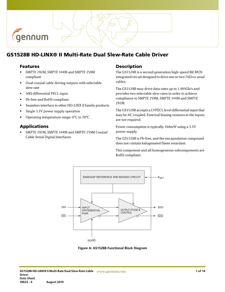
BANDGAP REFERENCE AND BIASING CIRCUIT
DDI
INPUT
DIFFERENTIAL
PAIR
RSET
SDO
OUTPUT STAGE &
CONTROL
DDI
SDO
SD/HD
Figure A: GS1528B Functional Block Diagram
GS1528B HD-LINX® II Multi-Rate Dual Slew-Rate Cable
Driver
Data Sheet
39623 - 4
August 2010
www.gennum.com
1 of 14
Revision History
Version
ECR
PCN
Date
4
154633
–
August 2010
3
153754
–
November 2009
2
142319
–
April 2007
1
141659
–
August 2006
0
140615
–
May 2006
Changes and/or Modifications
Correction to 7.1 Package Dimensions. Added 250pc tape & reel part number
to 7.4 Ordering Information.
Updated to latest Gennum template.
Converting to Data Sheet. Added section 7.3 Marking Diagram. Added
typical ORL value in Table 2-3: AC Electrical Characteristics.
Removed power consumption and supply current data for SDO/SDO disabled
in Table 2-2: DC Electrical Characteristics.
New document.
Contents
Features.................................................................................................................................................................1
Applications.........................................................................................................................................................1
Description...........................................................................................................................................................1
Revision History .................................................................................................................................................2
1. Pin Out...............................................................................................................................................................3
1.1 GS1528B Pin Assignment ...............................................................................................................3
1.2 GS1528B Pin Descriptions .............................................................................................................3
2. Electrical Characteristics ............................................................................................................................4
2.1 Absolute Maximum Ratings ..........................................................................................................4
2.2 DC Electrical Characteristics ........................................................................................................4
2.3 AC Electrical Characteristics ........................................................................................................5
3. Solder Reflow Profiles..................................................................................................................................6
4. Input / Output Circuits ................................................................................................................................7
5. Detailed Description.....................................................................................................................................8
5.1 Input Interfacing ...............................................................................................................................8
5.2 Output Interfacing ...........................................................................................................................8
5.3 Output Return Loss Measurement ........................................................................................... 10
5.4 Output Amplitude Adjustment ................................................................................................. 10
6. Application Information .......................................................................................................................... 11
6.1 PCB Layout ....................................................................................................................................... 11
6.2 Typical Application Circuit ........................................................................................................ 11
7. Package and Ordering Information...................................................................................................... 12
7.1 Package Dimensions ..................................................................................................................... 12
7.2 Packaging Data ............................................................................................................................... 12
7.3 Marking Diagram ........................................................................................................................... 13
7.4 Ordering Information ................................................................................................................... 13
GS1528B HD-LINX® II Multi-Rate Dual Slew-Rate Cable
Driver
Data Sheet
39623 - 4
August 2010
2 of 14
1. Pin Out
1.1 GS1528B Pin Assignment
DDI
1
DDI
2
VEE
3
RSET
4
GS1528B
8-PIN SOIC
TOP VIEW
8
SDO
7
SDO
6
SD/HD
5
VCC
Figure 1-1: 8-Pin SOIC
1.2 GS1528B Pin Descriptions
Table 1-1: Pin Descriptions
Pin Number
Name
Timing
Type
Description
DDI, DDI
Analog
Input
Serial digital differential input.
3
VEE
–
Power
Most negative power supply connection. Connect to GND.
4
RSET
Analog
Input
External output amplitude control resistor.
5
VCC
–
Power
Most positive power supply connection. Connect to +3.3V.
6
SD/HD
Non
Synchronous
Input
Output slew rate control. When set HIGH, the output will meet
SMPTE 259M rise/fall time specifications. When set LOW, the serial
outputs will meet SMPTE 292M rise/fall time specifications.
1,2
GS1528B HD-LINX® II Multi-Rate Dual Slew-Rate Cable
Driver
Data Sheet
39623 - 4
August 2010
3 of 14
2. Electrical Characteristics
2.1 Absolute Maximum Ratings
Table 2-1 lists the absolute maximum ratings for the GS1528B. Conditions exceeding the
limits listed may cause permanent damage to the device. This is a stress rating only and
functional operation of the device at these or any other conditions above those listed in
the operational sections of this specification is not implied. Exposure to absolute
maximum rating conditions for extended periods may affect device reliability.
Table 2-1: Absolute Maximum Ratings
Parameter
Value
Supply Voltage
-0.5V to 3.6 VDC
Input ESD Voltage
4kV
Storage Temperature Range
-50°C < Ts < 125°C
Input Voltage Range (any input)
-0.3 to (VCC +0.3)V
Operating Temperature Range
0°C to 70°C
Solder Reflow Temperature
260°C
Power Dissipation
300mW
2.2 DC Electrical Characteristics
Table 2-2 shows the DC electrical characteristics of the GS1528B where conditions are
VCC = 3.3V ±5%, TA = 0°C to 70°C, unless otherwise shown.
Table 2-2: DC Electrical Characteristics
Parameter
Symbol
Conditions
Min
Typ
Max
Units
Supply Voltage
VCC
–
3.135
3.3
3.465
V
Power Consumption
PD
TA = 25°C
–
168
–
mW
Supply Current
Is
TA = 25°C
–
51
64
mA
Output Voltage
VCMOUT
Common mode
–
VCC - VOUT
–
V
VCMIN
Common mode
1.4 +
ΔVDDI/2
–
VCC ΔVDDI/2
V
VIH
IIH <= 10uA
2.0
–
–
V
VIL
IIL <= 10uA
–
–
0.8
V
Input Voltage
SD/HD Input
GS1528B HD-LINX® II Multi-Rate Dual Slew-Rate Cable
Driver
Data Sheet
39623 - 4
August 2010
4 of 14
2.3 AC Electrical Characteristics
Table 2-3 shows the AC electrical characteristics of the GS1528B where conditions are
VCC = 3.3V ±5%, TA = 0°C to 70°C, unless otherwise shown.
Table 2-3: AC Electrical Characteristics
Parameter
Symbol
Conditions
Min
Typ
Max
Units
Notes
DRSDO
–
–
–
1.485
Gb/s
1
–
1.485Gb/s
–
20
–
psp-p
–
–
270Mb/s
–
16
–
psp-p
–
tr, tf
SD/HD=0
–
–
220
ps
2
tr, tf
SD/HD=1
400
–
800
ps
2
Utr, Utf
–
–
–
30
ps
–
–
SD/HD=0
–
–
30
ps
3
–
SD/HD=1
–
–
100
ps
3
–
SD/HD=0
–
–
10
%
3
–
SD/HD=1
–
–
8
%
3
Output Return Loss
ORL
–
15
20
–
dB
4
Output Voltage Swing
VOUT
RSET = 750Ω
750
800
850
mVp-p
3
UVDDI
Differential
300
–
2200
mVp-p
–
Serial input data rate
Additive jitter
Rise/Fall time
Mismatch in rise/fall time
Duty cycle distortion
Overshoot
Input Voltage Swing
NOTES:
1.
2.
3.
4.
The input coupling capacitor must be set accordingly for lower data rates.
Rise/Fall time measured between 20% and 80%.
Single Ended into 75Ω external load.
ORL depends on board design. The GS1528B achieves this specification on Gennum's evaluation boards.
GS1528B HD-LINX® II Multi-Rate Dual Slew-Rate Cable
Driver
Data Sheet
39623 - 4
August 2010
5 of 14
3. Solder Reflow Profiles
The device is manufactured with Matte-Sn terminations and is compatible with both
standard eutectic and Pb-free solder reflow profiles. MSL qualification was performed
using the maximum Pb-free reflow profile shown in Figure 3-1. The recommended
standard Pb reflow profile is shown in Figure 3-2.
Temperature
60-150 sec.
20-40 sec.
260°C
250°C
3°C/sec max
217°C
6°C/sec max
200°C
150°C
25°C
Time
60-180 sec. max
8 min. max
Figure 3-1: Maximum Pb-free Solder Reflow Profile (Preferred)
60-150 sec.
Temperature
10-20 sec.
230°C
220°C
3°C/sec max
183°C
6°C/sec max
150°C
100°C
25°C
Time
120 sec. max
6 min. max
Figure 3-2: Standard Pb Reflow Profile
GS1528B HD-LINX® II Multi-Rate Dual Slew-Rate Cable
Driver
Data Sheet
39623 - 4
August 2010
6 of 14
4. Input / Output Circuits
VCC
DDI
DDI
VCC
10k
5k
10k
10k
Figure 4-1: Differential Input Stage (DDI/DDI)
Vcc
SDO SDO
IREF
Figure 4-2: Differential Output Stage (SDO/SDO) IREF Derived Using RSET
VCC
SD/HD
On Chip
Reference
Figure 4-3: Slew Rate Select Input Stage
GS1528B HD-LINX® II Multi-Rate Dual Slew-Rate Cable
Driver
Data Sheet
39623 - 4
August 2010
7 of 14
5. Detailed Description
5.1 Input Interfacing
DDI/DDI are high impedance differential inputs. The equivalent input circuit is shown in
Figure 4-1.
Several conditions must be observed when interfacing to these inputs:
•
The differential input signal amplitude must be between 300 and 2200mVpp.
•
The common mode voltage range must be as specified in the Table 2.2.
•
For input trace lengths longer than approximately 1cm, the inputs should be
terminated as shown in the Typical Application Circuit.
The GS1528B inputs are self-biased, allowing for simple AC coupling to the device. For
serial digital video, a minimum capacitor value of 4.7μF should be used to allow
coupling of pathological test signals. A tantalum capacitor is recommended.
SD/HD Input Pin
The GS1528B SDO rise and fall times can be set to comply with both SMPTE 259M/344M
and SMPTE 292M. For all SMPTE 259M standards, or any data rate that requires longer
rise and fall time characteristics, the SD/HD pin must be set HIGH by the application
layer. For SMPTE 292M standards and signals which require faster rise and fall times,
this pin should be set LOW.
5.2 Output Interfacing
The GS1528B outputs are current mode, and will drive 800mV into a 75Ω load. These
outputs are protected from accidental static damage with internal ESD protection
diodes.
The SMPTE 292M, SMPTE 344M and SMPTE 259M standards require that the output of a
cable driver have a source impedance of 75Ω and a return loss of at least 15dB between
5MHz and 1.485GHz.
In order for a DDI output circuit using the GS1528B to meet this specification, the output
application circuit shown in the Typical Application Circuit on page 11 is
recommended.
The value of LCOMP will vary depending on the PCB layout, with a typical value of 5.6nH.
A 4.7μF capacitor is used for AC coupling the output of the device. This value is chosen
to ensure that pathological signals can be coupled without a significant DC component
occurring. Please see Application Information on page 11 for more details.
GS1528B HD-LINX® II Multi-Rate Dual Slew-Rate Cable
Driver
Data Sheet
39623 - 4
August 2010
8 of 14
Tek Stopped:
8110 Acquisitions
Figure 5-1: Output signal for 270Mb/s input
Tek Running: Normal
Figure 5-2: Output signal for 1.485Gb/s input
The output protection diodes act as a varactor (voltage controlled capacitor) as shown in
Figure 5-3. Therefore, when measuring return loss at the GS1528B output, it is necessary
to take the measurement for both a logic high and a logic low output condition.
Consequently, the output capacitance of the device is dependent on the logic state of the
output.
GS1528B HD-LINX® II Multi-Rate Dual Slew-Rate Cable
Driver
Data Sheet
39623 - 4
August 2010
9 of 14
GS1528B
SDO
SDO
Figure 5-3: Static Protection Diodes
5.3 Output Return Loss Measurement
To perform a practical return loss measurement, it is necessary to force the GS1528B
output to a DC high or low condition. The actual measured return loss will be based on
the outputs being static at VCC or VCC-1.6V. Under normal operating conditions the
outputs of the device swing between VCC-0.4V and VCC-1.2V.
5.4 Output Amplitude Adjustment
The output amplitude of the GS1528B can be adjusted by changing the value of the RSET
resistor as shown in Table 5-1. For an 800mVp-p output with a nominal ±7% tolerance, a
value of 750Ω is required. A ±1% SMT resistor should be used.
The RSET resistor is part of the high speed output circuit of the GS1528B. The resistor
should be placed as close as possible to the RSET pin. In addition, the PCB capacitance
should be minimized at this node by removing the PCB groundplane beneath the RSET
resistor and the RSET pin.
Table 5-1: RSET vs VOD
RSET R (Ω)
Output Swing (mVp-p)
995
608
824
734
750
800
680
884
573
1040
NOTE: For reliable operation of the GS1528B over the full temperature range, do not use an
RSET value below 573Ω.
GS1528B HD-LINX® II Multi-Rate Dual Slew-Rate Cable
Driver
Data Sheet
39623 - 4
August 2010
10 of 14
6. Application Information
6.1 PCB Layout
Special attention must be paid to component layout when designing serial digital
interfaces for HDTV.
An FR-4 dielectric can be used, however, controlled impedance transmission lines are
required for PCB traces longer than approximately 1cm. Note the following PCB artwork
features used to optimize performance:
•
The PCB trace width for HD rate signals is closely matched to SMT component
width to minimize reflections due to changes in trace impedance.
•
The PCB groundplane is removed under the GS1528B output components to
minimize parasitic capacitance.
•
The PCB ground plane is removed under the GS1528B RSET pin and resistor to
minimize parasitic capacitance.
•
Input and output BNC connectors are surface mounted in-line to eliminate a
transmission line stub caused by a BNC mounting via high speed traces which are
curved to minimize impedance variations due to change of PCB trace width.
6.2 Typical Application Circuit
*
5.6n
75
4u7
GS1528B
49.9
10n
1
2
3
49.9
4u7
4
8
7
6
75
10n
75
75
VCC
RSET
DIFFERENTIAL
DATA INPUT
VCC
SDO
SDO
SD/HD
DDI
DDI
VEE
BNC
4u7
BNC
*
5.6n
5
4u7
VCC
* TYPICAL VALUE VARIES WITH LAYOUT
VCC
750
10n
SD/HD
NOTE: All resistors in Ohms, capacitors in Farads,
and inductors in Henrys, unless otherwise noted.
Figure 6-1: GS1528B Typical Application Circuit
GS1528B HD-LINX® II Multi-Rate Dual Slew-Rate Cable
Driver
Data Sheet
39623 - 4
August 2010
11 of 14
7. Package and Ordering Information
D
X
E
0.010
Gauge Plane
Pin 1
ID Mark
q2
e
B
Seating Plane
L
DETAIL “A”
DETAIL “A”
0.015 ±0.004 x 45°
SYMBOL
7.1 Package Dimensions
Min.
Max.
A
0.054
A1
B
0.004
0.068
0.0098
D
E
H
e
0.196
0.157
0.244
0.229
0.050 BSC
C
L
C
A
q1
X
q1
q2
A1
8 SOIC
0.014
0.189
0.150
0.019
0.0075
0.016
0.0098
0.034
0.0215 REF
0°
8°
7° BSC
NOTES:
1. All dimensions in inches unless otherwise stated.
2. Lead coplanarity should be 0 to 0.004” max.
3. Package surface finishing: VDI 24~27 (dual).
Package surface finishing: VDI 13~15 (16L SOIC[NB] matrix).
4. All dimensions exclude mold flashes.
5. The lead width (B) to be determined at 0.0075”
from the lead tip.
Figure 7-1: GS1528B Package Dimensions
7.2 Packaging Data
Table 7-1: Packaging Data
Parameter
Value
Package Type
8-pin SOIC
Moisture Sensitivity Level
2
Junction to Case Thermal Resistance, θj-c
72°C/W
Junction to Air Thermal Resistance, θj-a (at zero airflow)
116°C/W
Pb-free and RoHS Compliant
Yes
GS1528B HD-LINX® II Multi-Rate Dual Slew-Rate Cable
Driver
Data Sheet
39623 - 4
August 2010
12 of 14
7.3 Marking Diagram
G
GS1528B
XXXXE3
YYWW
XXXX - Lot/Work Order ID
YYWW - Date Code
YY 2-digit year
WW 2-digit week number
Figure 7-2: GS1528B Marking Diagram
7.4 Ordering Information
Table 7-2: Ordering Information
Part Number
Package
Temperature Range
GS1528B
GS1528BCKAE3
8-pin SOIC
0°C to 70°C
GS1528B
GS1528BCTAE3
250pc tape & reel
8-pin SOIC
0°C to 70°C
GS1528B HD-LINX® II Multi-Rate Dual Slew-Rate Cable
Driver
Data Sheet
39623 - 4
August 2010
13 of 14
DOCUMENT IDENTIFICATION
CAUTION
DATA SHEET
ELECTROSTATIC SENSITIVE DEVICES
The product is in production. Gennum reserves the right to make changes to
the product at any time without notice to improve reliability, function or
design, in order to provide the best product possible.
DO NOT OPEN PACKAGES OR HANDLE EXCEPT AT A
STATIC-FREE WORKSTATION
GENNUM CORPORATE HEADQUARTERS
Phone: +1 (905) 632-2996
Fax: +1 (905) 632-2055
4281 Harvester Road, Burlington, Ontario L7L 5M4 Canada
E-mail: corporate@gennum.com
www.gennum.com
OTTAWA
SNOWBUSH IP - A DIVISION OF GENNUM
GERMANY
232 Herzberg Road, Suite 101
Kanata, Ontario K2K 2A1
Canada
439 University Ave. Suite 1700
Toronto, Ontario M5G 1Y8
Canada
Hainbuchenstraße 2
80935 Muenchen (Munich), Germany
Phone: +1 (613) 270-0458
Phone: +1 (416) 925-5643
Fax: +49-89-35804653
Fax: +1 (613) 270-0429
Fax: +1 (416) 925-0581
E-mail: gennum-germany@gennum.com
CALGARY
E-mail: sales@snowbush.com
3553 - 31st St. N.W., Suite 210
Calgary, Alberta T2L 2K7
Canada
Web Site: http://www.snowbush.com
Phone: +1 (403) 284-2672
UNITED KINGDOM
North Building, Walden Court
Parsonage Lane,
Bishop’s Stortford Hertfordshire, CM23 5DB
United Kingdom
MEXICO
288-A Paseo de Maravillas
Jesus Ma., Aguascalientes
Mexico 20900
Phone: +49-89-35831696
NORTH AMERICA WESTERN REGION
691 South Milpitas Blvd., Suite #200
Milpitas, CA 95035
United States
Phone: +1 (408) 934-1301
Fax: +1 (408) 934-1029
Phone: +1 (416) 848-0328
E-mail: naw_sales@gennum.com
JAPAN KK
NORTH AMERICA EASTERN REGION
Fax: +44 1279 714171
Shinjuku Green Tower Building 27F
6-14-1, Nishi Shinjuku
Shinjuku-ku, Tokyo, 160-0023
Japan
INDIA
Phone: +81 (03) 3349-5501
#208(A), Nirmala Plaza,
Airport Road, Forest Park Square
Bhubaneswar 751009
India
Fax: +81 (03) 3349-5505
Web Site: http://www.gennum.co.jp
KOREA
Phone: +91 (674) 653-4815
TAIWAN
Fax: +91 (674) 259-5733
6F-4, No.51, Sec.2, Keelung Rd.
Sinyi District, Taipei City 11502
Taiwan R.O.C.
8F Jinnex Lakeview Bldg.
65-2, Bangidong, Songpagu
Seoul, Korea 138-828
Phone: +44 1279 714170
E-mail: gennum-japan@gennum.com
Phone: (886) 2-8732-8879
Fax: (886) 2-8732-8870
4281 Harvester Road
Burlington, Ontario L7L 5M4
Canada
Phone: +1 (905) 632-2996
Fax: +1 (905) 632-2055
E-mail: nae_sales@gennum.com
Phone: +82-2-414-2991
Fax: +82-2-414-2998
E-mail: gennum-korea@gennum.com
E-mail: gennum-taiwan@gennum.com
Gennum Corporation assumes no liability for any errors or omissions in this document, or for the use of the circuits or devices described herein. The sale of
the circuit or device described herein does not imply any patent license, and Gennum makes no representation that the circuit or device is free from patent
infringement.
All other trademarks mentioned are the properties of their respective owners.
GENNUM and the Gennum logo are registered trademarks of Gennum Corporation.
© Copyright 2004 Gennum Corporation. All rights reserved.
www.gennum.com
GS1528B HD-LINX® II Multi-Rate Dual Slew-Rate Cable
Driver
Data Sheet
39623 - 4
August 2010
14 of 14
14
