ISSN: 2278 – 1323
International Journal of Advanced Research in Computer Engineering & Technology (IJARCET)
Volume 2, Issue 11, November 2013
A review and Exploration of various Elements
Inducing noise in Scheming Instrumentation
amplifier
P.ARUMBU, V.ANAND, B.KARTHIK, V.GOPI
Abstract—The objective of the paper is to propose the Noise
model of a three op-amp instrumentation amplifier focusing
the noise awareness features to be considered when designing
the instrumentation amplifier to sense and amplify low voltages
which
finds
delicate
application
like
biomedical
instrumentation. Change of gain and CMRR (Common mode
rejection ratio) due to unexpected reaction from the
environment and tolerance value of the externally connected
components are considered and discussed in detail. Impact
factors like temperature and gain in Amplification of noise are
also taken as factors while calculating Total Noise and tried to
simulate with Cadence tool for Analog and Mixed signal
analysis. This paper is intended as a step to analyze the noise
there by incorporate suitable safety measurements to optimize
the accuracy of Output while using the instrumentation
amplifier as signal conditioning circuits in sensitive signal
measurements in future.
Index Terms— Tolerance, gain, CMRR, Temperature, Noise
Model, accuracy.
I. INTRODUCTION
When considering the instrumentation amplifier as a part of
data acquisition system in biomedical instrumentation the
main factor to be considered is accuracy, because the
Electrodes or sensor in the outer skin of human body detect
the small voltages according to the function of organs in the
order of 1 micro volt to hundreds of microvolt. But the signal
is too small and contains a lot of added noise [1], [2]. For an
example Fig.1 showsThe small
electrical signal from the heart
generates a common-mode voltage
and noise in the system. The
signals from the heart are too
small and it is necessary to amplify
the signal and reduce the
common-mode voltage on the system. Other aspects that
generate noise are muscle Contractions, respiration,
Electromagnetic interference and
Electromagnetic
emissions from electronic components. The signal has
amplitude of approximately 1 mV peak to peak and contains
common-mode voltage noises. While processing a low
amplitude signal and accuracy is a key factor to be fulfilled
the various causes that deviates the optimum value of
accuracy in the data acquisition system are essential to find
out results scheming of low noise instrumentation amplifier.
A low noise instrumentation amplifier is an extremely
sensitive device that can measure even the smallest signals in
noisy environments or in the presence of large unwanted
voltages. In order to process the low voltage signals the
instrumentation amplifier must have high common mode
rejection ratio. The instrumentation amplifier with high
CMRR cancels the noise appearing commonly at their input
terminals and increases the likelihood to amplify the low
voltage input signals more accurately. A low noise
instrumentation amplifier combines a very low wideband
Noise with a low 1/f corner [3] which makes it useful in the
most demanding precision applications that too while
measuring bio-signals the amplifier, has to satisfy few
requirements such as (i) The low noise instrumentation
amplifier must provide best isolation between signal and
noise.(ii) It has to provide the electrical isolation between
patient and device. (iii) It should not affect the process to be
monitored and should not alter the function in any way. (iv)It
has to provide at most accurate result. (v)It has to tolerate the
fluctuations in the input and protect the instrument in case of
high input voltage occurred suddenly.
Basic configuration
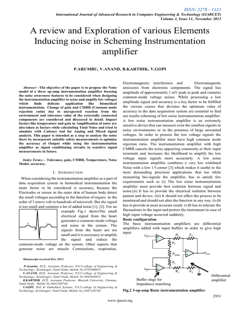
The basic instrumentation amplifiers are differential
amplifiers added with input buffers in order to give high
input
Manuscript received Oct, 2013.
P.Arumbu, ECE, Assistant Professor, P.S.V.college of Engineering &
Technology,, Krishnagiri, Tamil Nadu, Mobile No 9791900035.
V.ANAND, ECE, Assistant Professor, P.S.V.college of Engineering &
Technology,, Krishnagiri, Tamil Nadu, Mobile No 9943944022.
B.KARTHIK, ECE, Assistant Professor, Bharath University, Chennai,
Tamil Nadu, Mobile No.9842580740,
V.GOPI, M.E In Embedded Systems, P.S.V.college of Engineering &
Technology, Krishnagiri, Tamil Nadu, Mobile No.,9487326748
Buffer stage for
Impedance matching
Differential
amplifier
Fig.2 3-op-amp Basic instrumentation amplifier
2951
www.ijarcet.org
ISSN: 2278 – 1323
International Journal of Advanced Research in Computer Engineering & Technology (IJARCET)
Volume 2, Issue 11, November 2013
impedance. The gain of the circuit is
The differential amplifier has the ability to reject the
common signals appearing at its both inverting and
non-inverting terminals and senses the small difference in
signal across its input terminals and amplifies based on the
gain. By taking proper corrective measurements and
considering design parameters it is possible to provide high
signal to noise ratio and eliminate the interferences raised
magnetically or electrostatically
II. CALCULATION OF DESIRABLE VALUE OF CMRR IN LOW
AMPLITUDE APPLICATIONS
In order to identify even a very smaller difference of signal
across the input terminals, the ideal instrumentation
amplifier must have infinite CMRR value.
The dB value of CMRR is given as
-----> (1)
Ad =differential mode gain
Acm =common mode gain. For common noise signal
appearing at the both of input terminals the gain should be
zero for optimum accuracy. It requires a very high degree of
resistance value matching, but due to tolerance value of
resistors generally the CMRR will not be infinite.
R2
R1
V-
OPAMP
OUT
R3
reference of Bio medical applications it has been identified
that the minimum CMRR is100dB to handle low voltage
signals.[2]
Referring equation (1)
=100dB
Consider differential mode gain (Ad) =1; above
expression turns as
Maximum common mode gain should be Acm = 0.00001
to satisfy the minimum requirement of 100dB or in other
terms the noise amplification factor must be lesser than to
meet the application demands while measuring low
amplitude signals.
III. A SIMPLE NOISE MODEL OF AN INSTRUMENTATION
AMPLIFIER
The three main noise sources of instrumentation amplifier
are (i) Voltage noise (ii) Current Noise (iii) Thermal Noise
on source resistance. These noise sources are totally un
correlated. The term source resistance takes the account of
externally connected resistors and internal resistance of the
sensor connected at the input terminals of Op-amp. The
externally connected resistors match the input impedance of
the circuit. Voltage noise can be classified as Input voltage
noise (ei) output voltage noise (eo).
The rms (root mean square) value of source resistance is
+
0
V+
Volts.
Where k = Boltzmann’s constant, T=absolute temperature,
Rs= total source resistance and B=Bandwidth in Hz.
R4
0
Vref
0
Fig.3 Differential amplifier
Interms of resistors the CMRR of a differential amplifier is
represented by referring fig.3 as
CMRR =
Where
----> (2)
The influency of tolerance value of resistors over the CMRR
at various gain values specified in an application note of
Intersil Corporation is given in Table 1.
RESISTOR
CMRR
TOLERANCE
GAIN 1
GAIN 10
GAIN 100
±5%
-20.4dB
-15.6dB
-14.8dB
±1%
-34.1dB
-28.9dB
-28.1dB
±0.1%
-54.0dB
-48.8dB
-40.0dB
The total input noise
+
Throughout the bandwidth
the total input noise
is also designated as referred to input or RTI noise signified
in the unit of
given as
±0.01%
-74.0dB -68.8dB
-68.0dB
TABLE 1 Resistors over CMRR at various gain values
From Table 1. Designing the Instrumentation amplifier
with the resistors of lower tolerance value increases the
CMRR. But the other side the requirement of High gain of
the amplifier lowers the CMRR. So it is evident that the
calculation of minimum CMRR to reject interferences in
order to handle low voltage signals required. From the
All Rights Reserved © 2013 IJARCET
2952
ISSN: 2278 – 1323
International Journal of Advanced Research in Computer Engineering & Technology (IJARCET)
Volume 2, Issue 11, November 2013
V. IN-AMPS VERSUS OP-AMPS
Fig.4 Simple noise model of instrumentation amplifier
The source resistance includes the following noises. (i)
Thermal noise (ii) Contact Noise (iii) Johnson noise (iv)
Parasitic noise. Among above noises the Johnson noise
increases with square root of the resistance. A 1kΏ resistor
has4
approximately at room temperature, but for
highest performance amplifiers should have 1
as
total voltage noise [4]. These resistive noise sources can be
decreased by selecting an amplifier which has negligible
noise affect than source resistance noise, connecting external
resistors of minimum value and low noise contribution. They
can also be reduced by compromising the range of operating
frequency of an amplifier.
IV. CATEGORIES OF INTERNAL AMPLIFIER NOISE
The noise sources of Op-amp have Random behavior can
be formulated by Gaussian distribution. The noises are
generally unrelated so it is useful that inclusive of correlated
coefficient factor. The correlated noise is discarded if it lies
between the ranges of 10-15%. The internal noise of O-amp
can be classified as follows(i) input referred voltage noise
,discussed in chapter III.(ii) input referred current noise.(iii)
flicker noise and (iv) popcorn noise.
Input referred current noise:
Shot noise or schottky noise is referred as current noise due to
random flow of charge carriers during current flow. This can
be computed through the formula
Where
IB-Bias current in ampere(A), q-electron charge in coulomb
and B-Bandwidth in Hz.
Flicker noise:
The noise of op-amp is Gaussian with constant spectral
density or white noise over wide range of frequencies. But
when the frequency decreases spectral density starts to rise
because of the fabrication process. This low frequency noise
characteristic is known as Flicker noise. Bipolar and JFET
amplifiers have low corner frequency than CMOS amplifiers.
Popcorn noise:
A sudden shift of offset voltage or current from several µV to
hundreds of µV for few milliseconds due to contamination or
silicon surface defects is called popcorn noise. The desirable
situation for popcorn noise is low temperature and high
source resistance.
However the interference of noise can be minimized by
proper layout techniques to avoid parasitics, proper
grounding and by proper shielding.
Fig.5 In-Amp circuit
In Op-amps (Operational amplifiers) the closed loop gain is
determined by the externally connected resistor across the
non-inverting input terminal and Output pins. But the
specially designed In-Amps or instrumentation amplifier the
gain resistor is integrated internally or can be connected
externally; in both the cases the gain resistor is isolated from
input signal.
In-amp circuit has integrated buffer and gain stage makes
less requirement to externally connected resistors there by
reduces total source resistance that produces noise.
Fig.6 Op-amp circuit
Because of less or no external resistors the RTI (Referred to
Input noise) equation of In-Amps are given as
With input Bias current compensation the total voltage noise
can be reduced to 8
.
Noise model of In-Amp
Fig.7 Noise model of In-amp
Where Rs is the source resistance, VNI is the Input noise
voltage which is appeared at the input terminals and
2953
www.ijarcet.org
ISSN: 2278 – 1323
International Journal of Advanced Research in Computer Engineering & Technology (IJARCET)
Volume 2, Issue 11, November 2013
amplified by gain G results output noise VNO. IN+ and IN- are
input noise current usually they are equal but uncorrelated.
The noise created by input noise current is INRs/2 in one
terminal. The total output noise is calculated by
The total input noise is calculated by
VI. CALCULATION OF OUTPUT NOISE USING ORCAD 16.6
The below figure.8 shows a 3 –op amp instrumentation
amplifier with externally connected resistors for input
impedance matching and gain. In order to calculate the
interference of noise in the input terminal and its value after
amplification at the output input voltages are connected to
ground. Total noise voltage is calculated for various gain and
in various temperature using OrCAD 16.6. It is a tool set for
windows application, can be used to simulate analog and
mixed signal circuits.
V1
0Vac
0Vdc
U1
0V
+
R6
0
OUT
-
OPAMP
0V
R2
R1
1.5k
1k
10k
OPAMP
R7
1k
V
+
U3
R4
1.5k
OPAMP
OUT
0V
R3
-
0V
V
1k
R5
10k
V
0V
0V
0
OUT
V2
0Vac
0Vdc
(1)
+
U2
0V
0V
0
Fig.8 Simulated 3 op-amp instrumentation amplifier
(2)
pSPICE CODING OF ABOVE
INSTRUMENTATION AMPLIFIER
for ac sweep &NOISE ANALYSIS
.lib "nomd.lib"
*Analysis directives:
.AC DEC 10khz 100khz 10Ghz
.NOISE v(E_U3) V_V1 1
.OPTIONS ADVCONV
.PROBE64 V(alias(*)) I(alias(*)) W(alias(*)) D(alias(*))
NOISE(alias(*))
.INC "..\SCHEMATIC1.net"
**** INCLUDING SCHEMATIC1.net ****
* source IA7
E_U1
N00212 0 VALUE
{LIMIT(V(N00437,N00203)*1E6,-15V,+15V)}
E_U2
N00256 0 VALUE
{LIMIT(V(N00611,N00260)*1E6,-15V,+15V)}
E_U3
N00239 0 VALUE
{LIMIT(V(N00269,N00216)*1E6,-15V,+15V)}
R_R1
N00212 N00216 1k TC=0,0
R_R2
N00203 N00212 1.5k TC=0,0
R_R3
N00260 N00256 1.5k TC=0,0
R_R4
N00256 N00269 1k TC=0,0
R_R5
0 N00269 10k TC=0,0
R_R6
N00239 N00216 10k TC=0,0
R_R7
N00203 N00260 1k TC=0,0
V_V1
N00437 0 DC 0Vdc AC 0Vac
V_V2
N00611 0 DC 0Vdc AC 0Vac
**** RESUMING IA7.cir ****
.END
RESULT: at 27C and Gain =10
TOTAL OUTPUT NOISE VOLTAGE
= 2.354E-14 (SQ
V/HZ)
EQUIVALENT INPUT NOISE ATV_V1
= 3.835E-09
(V/RT HZ)
CODINGS FOR TRANSIENT ANALYSIS
.lib "nomd.lib"
*Analysis directives:
.TRAN 0 1000us 0 10us
.OPTIONS ADVCONV
.PROBE64 V(alias(*)) I(alias(*)) W(alias(*)) D(alias(*))
NOISE(alias(*))
.INC "..\SCHEMATIC1.net"
**** INCLUDING SCHEMATIC1.net ****
* source SAMPLE7
E_U1 0V
N00212 0 VALUE
{LIMIT(V(N00437,N00203)*1E6,-15V,+15V)}
E_U2
N00256 0 VALUE
{LIMIT(V(N00611,N00260)*1E6,-15V,+15V)}
E_U3
N00239 0 VALUE
{LIMIT(V(N00269,N00216)*1E6,-15V,+15V)}
R_R1
N00212 N00216 1k TC=0,0
R_R2
N00203 N00212 1.5k TC=0,0
R_R3
N00260 N00256 1.5k TC=0,0
R_R4
N00256 N00269 1k TC=0,0
R_R5
0 N00269 10k TC=0,0
R_R6
N00239 N00216 10k TC=0,0
R_R7
N00203 N00260 1k TC=0,0
V_V1
N00437 0 0Vdc
V_V2
N00611 0 200mVdc
**** RESUMING IA7.cir ****
.END
RESULT: at 27C and Gain =10
Node number followed by voltage at node are given as
(N00203) 300.0E-09 (N00212) -.3000 (N00216) .4545
(N00239) 7.9999 (N00256) .5000 (N00260) .2000
(N00269) .4545 (N00437) 0.0000 (N00611) .2000
The above circuit is simulated for various gain values at
various temperatures in order to calculate the influence of
gain and temperature in noise amplification and values are
tabulated.
All Rights Reserved © 2013 IJARCET
2954
ISSN: 2278 – 1323
International Journal of Advanced Research in Computer Engineering & Technology (IJARCET)
Volume 2, Issue 11, November 2013
TOTAL VOLTAGE NOISE
GAIN =10
tem
pC
20
27
30
35
o/p noise
(V/RT Hz)
1.516E-07
1.534E-07
1.542E-07
1.554E-07
GAIN =100
i/p noise
(V/RT
Hz)
tem
pC
3.791E09
3.835E09
3.855E09
3.886E09
20
27
30
35
o/p noise
(SQ
V/HZ)
i/p noise
(V/RT
Hz)
1.506E-06
3.766E-09
1.524E-06
3.811E-09
1.532E-06
3.830E-09
1.544E-06
3.862E-09
TABLE 2.
.
VII. CONCLUSION
This paper consists of a 3 op-amp instrumentation model
and calculation of noise using a verification tool from
Cadence OrCad 16.6. Low noise instrumentation amplifiers
require precision amplification to meet the today’s
challenges in measuring low amplitude signals. The best
amplifier is not always the one with minimum
voltage noise. The gain, source resistance and frequency
range must be considered to find best amplifier. For low
value of source resistance voltage noise dominates and for
high value of source resistance current noise dominates.
Consider
and
.
If Source resistance Rs <RV Voltage noise dominates and
source resistance Rs>RI current noise dominates. For the
source value of 5kΏ to 10Ώ the noise performance of all the
instrumentation amplifiers are almost close to same. Under
such situation Bandwidth, power, distortion and cost are to
be considered as optimizing parameters.
P.ARUMBU Received B.E.S.degree from University of Madras, India in
1998. She received MSc degree from Bharathiar University in 2005, Mphil
degree from Bharathidasan university in 2008 and ME degree from
Sathyabama university in 2010. At present she is working as Assistant Professor
at P.S.V.college of Engineering & Technology and doing research in
Information and communication department under Anna University- Chennai..
V.ANAND Received the B.E degree from University of Madras, India in
2002. He received M.E degree from Anna University in 2004. At present he is
working as Assistant Professor at P.S.V.college of Engineering & Technology
and doing research in Mobile Communication & Embedded System under Anna
University-Chennai.
B.KARTHIK is an Assistant professor in the department of Electronics and
Communication Engineering, Bharath University, Chennai, India.. He received
his Master of Engineering in Applied Electronics in 2011. He is doing his
research work in Image Processing at Bharath University, Chennai, India. His
area of interests includes Image Processing, Network Security System
Techniques.
V.GOPI Received The B.E Degree From Anna University, In 2010.At
Studying I Year M.E In Embedded Systems Technologies. Of P.S.V.College Of
Engineering & Technology. And Doing Research In Wireless Communcations
REFERENCES
[1] Free scale Semiconductor Application Note Document Number:
AN4059 Rev. 0, 3/2010 “Heart Rate Monitor and Electrocardiograph
Fundamentals”- Carlos Casillas, RTAC Americas, Guadalajara, Mexico.
[2]. Nagel, J. H. “Biopotential Amplifiers.” The Biomedical Engineering
Handbook: Second Edition.Ed. Joseph D. Bronzino Boca Raton: CRC Press
LLC, 2000
[3]. Technical Article MS-2317”Designing High Performance Systems with
Low Noise Instrumentation Amplifiers” by Gustavo Castro, Applications
Engineer, Scott Hunt, Applications Engineer, Integrated Amplifier Products,
Analog Devices.
[4]” Low noise amplifier selection guide for optimal noise performance”-by
Paul Lee, Analog devices Application note AN-940.
[5]Designer’s guide to instrumentation amplifier. 3rd edition-Analog
devices.
2955
www.ijarcet.org


