Tutorial on Transistor Sizing Problem #1 (Static CMOS logic
advertisement
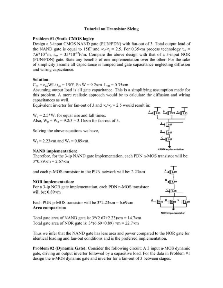
Tutorial on Transistor Sizing Problem #1 (Static CMOS logic): Design a 3-input CMOS NAND gate (PUN/PDN) with fan-out of 3. Total output load of the NAND gate is equal to 15fF and µn/µp = 2.5. For 0.35µm process technology tox = 7.6*10-9m, εox = 35*10-12F/m. Compare the above design with that of a 3-input NOR (PUN/PDN) gate. State any benefits of one implementation over the other. For the sake of simplicity assume all capacitance is lumped and gate capacitance neglecting diffusion and wiring capacitance. Solution: Cox = εoxWL/ tox = 15fF. So W = 9.2µm. Leff = 0.35µm. Assuming output load is all gate capacitance. This is a simplifying assumption made for this problem. A more realistic approach would be to calculate the diffusion and wiring capacitances as well. Equivalent inverter for fan-out of 3 and µn/µp = 2.5 would result in: Wp = 2.5*Wn for equal rise and fall times. Also, Wp + Wn = 9.2/3 = 3.16µm for fan-out of 3. A B 2.23 2.23 A Solving the above equations we have, 2.23 2.67 B 2.67 C Wp = 2.23µm and Wn = 0.89µm. C 2.67 NAND implementation NAND implementation: Therefore, for the 3-ip NAND gate implementation, each PDN n-MOS transistor will be: 3*0.89µm = 2.67µm and each p-MOS transistor in the PUN network will be: 2.23µm A NOR implementation: For a 3-ip NOR gate implementation, each PDN n-MOS transistor will be: 0.89µm B Each PUN p-MOS transistor will be 3*2.23µm = 6.69µm Area comparison: 6.69 C A 0.89 B 6.69 6.69 0.89 C 0.89 NOR implementation Total gate area of NAND gate is: 3*(2.67+2.23)µm = 14.7µm Total gate area of NOR gate is: 3*(6.69+0.89) µm = 22.7µm Thus we infer that the NAND gate has less area and power compared to the NOR gate for identical loading and fan-out conditions and is the preferred implementation. Problem #2 (Dynamic Gate): Consider the following circuit: A 3 input n-MOS dynamic gate, driving an output inverter followed by a capacitive load. For the data in Problem #1 design the n-MOS dynamic gate and inverter for a fan-out of 3 between stages. Solution: The total load being driven is equivalent to a transistor width of 9.2um. The load is driven by a dynamic gate followed by an inverter. The inverter size for a fan-out of 3 is equal to that in the above problem and is given by p-MOS = 2.23um and n-MOS = 0.89um. So, the total load being driven by the dynamic gate is equal to 3.16um. For a fan-out of 3, the equivalent width for the inverter representing the dynamic stage should be equal to 3.16/3 = 1.05um. Applying the same equations as in Problem #1, we have: p-MOS + n-MOS = 1.05um. p-MOS = 2.5n-MOS. So, 3.5n-MOS = 1.05/3.5um. n-MOS = 0.3um and p-MOS = 2.5*0.3um = 0.75um For the 3-input dynamic gate there are 4 n-MOS transistors in series. So, each n-MOS transistor is 4*0.3um = 1.2um Problem #3 (Transmission Gate): Consider a circuit as follows: An inverter driving a transmission gate driving a capacitive load (all three in series). Design the transmission gate and inverter when the lumped capacitive load is equal 30fF. In addition, assume that there is wiring capacitance of 15fF as well. Design the inverter for a fan-out of 2 for high performance. Assume µn = 0.04m2/Vs, µp = 0.016m2/Vs, Vtn = |Vtp| = 0.7, Vdd = 3.3V. Size the TG to ensure the equivalent RC delay to be equal to 18ps. Solution: Total capacitance at output of TG = load capacitance + wiring capacitance = 45fF. RC delay = 18ps implies that R = 18*10-12/45*10-15 = 400 Ohm Req = 1/[(kn(Vdd-Vtn) + kp(Vdd-|Vtp|)] Where kn = µnWnCox/L Substituting the given values from above in the equation, we obtain n-MOS = 0.89um and p-MOS = 2.23um. The inverter driving the TG and capacitive load sees a load equal to the diffusion capacitance of the TG + the capacitive load (9.2um). We assume that the diffusion capacitance of a transistor is approximately equal to 1/3 of its gate capacitance. Hence, the capacitive load offered by the TG = (p-MOS + n-MOS)/3 = 3.16/3 = 1.05um. Thus the total load at the output of the inverter = load of TG (1.05um) + load of output capacitance (9.2um) = 10.25um. The driving inverter needs to be designed for a fan-out of 2 for a total output load of 10.25um. Thus the p-MOS + n-MOS width of the inverter = 10.25/2 = 5.13um For equal rise and fall times, p-MOS = 2.5n-MOS. So, 3.5n-MOS = 5.13um, n-MOS = 1.47 and p-MOS = 2.5*1.47 = 3.68um
