Surface Mount Assembly Guidelines for Optical
Dual FlatPack No Lead (ODFN) Package
®
Technical Brief
March 14, 2008
TB466.1
Introduction
Part I - ODFN Board Mounting Guidelines
Optical Dual-in-line Flat No-lead (ODFN) packages are
developed for light sensor applications. The mechanical
structure of an ODFN is similar to that of a conventional
DFN, except the molding compound is a transparent
material rather than the conventional black compound.
Transparent molding compound allows transmission of
ambient light through the molding compound to reach the die
sensor area. The ODFN is a Pb-free package, with 100%
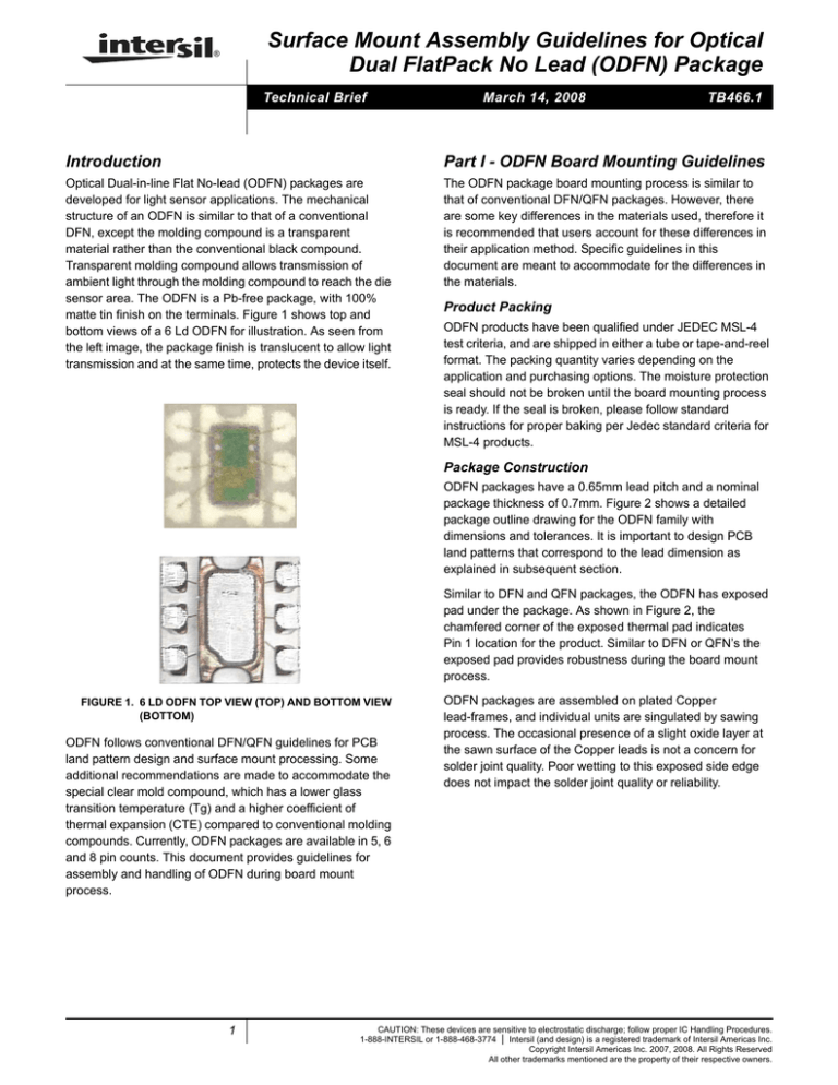
matte tin finish on the terminals. Figure 1 shows top and
bottom views of a 6 Ld ODFN for illustration. As seen from
the left image, the package finish is translucent to allow light
transmission and at the same time, protects the device itself.
The ODFN package board mounting process is similar to
that of conventional DFN/QFN packages. However, there
are some key differences in the materials used, therefore it
is recommended that users account for these differences in
their application method. Specific guidelines in this
document are meant to accommodate for the differences in
the materials.
Product Packing
ODFN products have been qualified under JEDEC MSL-4
test criteria, and are shipped in either a tube or tape-and-reel
format. The packing quantity varies depending on the
application and purchasing options. The moisture protection
seal should not be broken until the board mounting process
is ready. If the seal is broken, please follow standard
instructions for proper baking per Jedec standard criteria for
MSL-4 products.
Package Construction
ODFN packages have a 0.65mm lead pitch and a nominal
package thickness of 0.7mm. Figure 2 shows a detailed
package outline drawing for the ODFN family with
dimensions and tolerances. It is important to design PCB
land patterns that correspond to the lead dimension as
explained in subsequent section.
Similar to DFN and QFN packages, the ODFN has exposed
pad under the package. As shown in Figure 2, the
chamfered corner of the exposed thermal pad indicates
Pin 1 location for the product. Similar to DFN or QFN’s the
exposed pad provides robustness during the board mount
process.
FIGURE 1. 6 LD ODFN TOP VIEW (TOP) AND BOTTOM VIEW
(BOTTOM)
ODFN follows conventional DFN/QFN guidelines for PCB
land pattern design and surface mount processing. Some
additional recommendations are made to accommodate the
special clear mold compound, which has a lower glass
transition temperature (Tg) and a higher coefficient of
thermal expansion (CTE) compared to conventional molding
compounds. Currently, ODFN packages are available in 5, 6
and 8 pin counts. This document provides guidelines for
assembly and handling of ODFN during board mount
process.
1
ODFN packages are assembled on plated Copper
lead-frames, and individual units are singulated by sawing
process. The occasional presence of a slight oxide layer at
the sawn surface of the Copper leads is not a concern for
solder joint quality. Poor wetting to this exposed side edge
does not impact the solder joint quality or reliability.
CAUTION: These devices are sensitive to electrostatic discharge; follow proper IC Handling Procedures.
1-888-INTERSIL or 1-888-468-3774 | Intersil (and design) is a registered trademark of Intersil Americas Inc.
Copyright Intersil Americas Inc. 2007, 2008. All Rights Reserved
All other trademarks mentioned are the property of their respective owners.
Technical Brief 466
Optical Dual Flat No-Lead Family (ODFN)
0.10 C
2X
D
A
4
5
MDP0052
OPTICAL DUAL FLAT NO-LEAD FAMILY
4
0.10 C
2X
E
1
5
B
2
3
SYMBOL
ODFN5
ODFN6
ODFN8
TOLERANCE
A
0.70
0.70
0.70
±0.05
A1
0.02
0.02
0.02
+0.03/-0.02
b
0.30
0.30
0.30
±0.05
c
0.20
0.20
0.20
Reference
D
2.00
2.00
3.00
Basic
D2
1.35
1.35
2.29
Reference
E
2.10
2.10
3.00
Basic
E2
0.65
0.65
1.40
Reference
e
0.65
0.65
0.65
Basic
e1
1.30
1.30
1.95
Basic
L
0.35
0.35
0.40
±0.05
NOTE
2
TOP VIEW
3
(D2)
e1
4
5
L TYP.
3 (E2)
3
2
1
PIN
#1 I.D.
NOTES:
0.10
CA B
1. Dimensioning and tolerancing per ASME Y14.5M-1994.
2. Exposed lead at side of package is a non-functional feature.
BOTTOM VIEW
5 LD ODFN
(2.0x2.1 BODY)
3. Dimension D2 and E2 define the size of the exposed pad.
4. ODFN 5 Ld version has no center lead (shown as dashed line).
3
(D2)
e1
4 5
5
6
3
(D2)
e1
7
6
8
L TYP.
L TYP.
3 (E2)
3
3
2
(E2)
PIN
#1 I.D.
1
PIN
#1 I.D.
b
e
0.10
3
Rev. 4 5/06
b
e
3
CA B
4
e
3
2
1
b
0.10
BOTTOM VIEW
6 LD ODFN
(2.0x2.1 BODY)
CA B
BOTTOM VIEW
8 LD ODFN
(3.0x3.0 BODY)
0.10 C
C
SEATING
PLANE
C
0.08 C
(ALL LEADS
& EXPOSED PAD)
SEE
DETAIL "X"
SIDE VIEW
A
2
(C)
A1
DETAIL X
FIGURE 2. 5 LD ODFN, 6 LD ODFN AND 8 LD ODFN PACKAGE DIMENSIONS AND TOLERANCES
2
TB466.1
March 14, 2008
Technical Brief 466
6
1
(0 . 65)
PIN 1
INDEX AREA
(0 . 65)
0.65
1 . 35
(1 . 35)
1 . 30 REF
( 6X 0 . 30 )
( 6X 0 . 55 )
6X 0 . 30 ± 0 . 05
0 . 65
(1 . 95)
0.10 M C A B
6X 0 . 35 ± 0 . 05
BOTTOM VIEW
TYPICAL RECOMMENDED LAND PATTERN
FIGURE 3. 6 LD ODFN FOOTPRINT (LEFT) AND CORRESPONDING LAND PATTERN FOR PCB DESIGN (RIGHT)
PCB Land Pattern Design
The pad definition on the board is recommended to be
non-solder-mask-defined (NSMD), though
solder-mask-defined (SMD) pads of the same effective
wettable dimension are acceptable as well. A Nickel/Gold
surface finish with 0.2 micron maximum gold thicknesses is
recommended for good solder wettability and shelf-life for
the SMT process. OSP surface finish is also acceptable, but
requires appropriate controls on shelf life and exposure of
PCB to environment. HASL or solder plated finishes must
not be used for these products.
Intersil Technical Brief 389
http://www.intersil.com/design/packages/#TechBriefs
provides detailed information for PCB design for DFN and
QFN package, and this is applicable to ODFN packages.
Additionally, package specific land pattern information is
available on package outline drawings which are located on
the following website:
http://www.intersil.com/design/packages/
The package outline drawings are also found in product
datasheets. An example of land pattern recommendation is
shown in Figure 3 (6 Ld ODFN). The main features can be
summarized as follows:
Solder Stencil
Either 0.100mm or 0.125mm thick stainless steel stencil is
recommended.
The stencil should be laser-cut followed by electro-polish
(chemical finishing is not recommended), or alternatively an
additive build-up stencil may be used.
• 1:1 match with exposed pad area
(6 Ld ODFN case, 0.65mmx1.35mm)
• 1:1 match with pin width
(6 Ld ODFN case, 0.3mm)
Higher reliability on board can be obtained by increased
solder paste volumes. However, this needs to be controlled,
as solder bridging may occur when the solder paste is
excessive.
• Land length for pin = pin length + 0.2mm
(extended from the package edge)
Figure 4 shows a reference solder joint shape after ODFN
package mounting on PCB. Solder joint under the exposed
pad is intended to provide the package stand-off height and
robust assembly.
It is highly recommended to solder the exposed package pad
to the corresponding landing pad on the PCB. At the same
time, excessive solder under the exposed area may lead to
open solder joints under the functional pins due to excess
SENSOR
FILLET MAY OR MAY NOT FORM
DEPENDING ON OXIDATION
AT TRIMMED EDGE.
FIGURE 4. ODFN PACKAGE ON PCB WITH A REFERENCE SOLDER JOINT SHAPE
3
TB466.1
March 14, 2008
Technical Brief 466
Solder Paste
The package itself is lead-free, and is compatible with both
eutectic tin/lead or lead-free tin/silver/copper solders. These
packages have been qualified at a +240°C maximum
temperature reflow profile for eutectic solder, and at a
+260°C maximum temperature reflow profile for lead-free
solder. Solder paste with "no-clean" flux and "type 3" or "type
4" solder particle size distribution is recommended.
Reflow Profile
Direct infrared (IR) heating of these packages should not be
done as it can damage the part. Pure convection reflow of
these parts is recommended. Typical reflow profiles per
Jedec 20D criteria are recommended for the eutectic Sn/Pb
and lead-free Sn/Ag/Cu solders. Peak temperature for the
eutectic Sn/Pb profile is not to exceed +235°C and for the
lead-free profile is not to exceed +260°C respectively. ODFN
packages have been qualified up to a maximum reflow
temperature of +260°C
Sensor Location and Optics Design
In general, the package body center does not coincide with
the center of the light sensor. As shown in Figure 1 (top), the
sensor location (green area in top part of IC) is offset from the
geometric center of the IC. The location of the sensor itself is
specific to the product in question, and therefore should be
obtained from the product datasheet. Figure 5 shows an
example of the sensor location description. In this example,
the sensor area is 0.43mmx0.61mm, and it is offset from the
center of the IC by 0.25mm. The application set-up should be
designed to lead the light to the center of the sensor area and
not to the center of the package. On the other hand, the
sensor surface height is always located at 0.28 ±0.10mm
below the top surface of the package. Solder joint and
package height (0.7mm) should also be considered in
calculating the sensor surface height from the PCB top
surface.
ISL29001
(6 LD ODFN)
TOP VIEW
VDD
ODFN packages have been qualified up to a maximum
reflow temperature of +260°C.
1
6 SDA
GND 2
5 SCL
REXT 3
4 PD
Visual inspection of solder joints should be done to verify
that there is no solder bridging between pads, that the solder
joint is "bright-and-shiny" (lead-free appears 'dull' compared
to SnPb), and that the package is not tilted or off-center with
respect to the PCB land pattern. A solder fillet at the edge of
package leads is not a requirement, and in fact may not form
at all. Hand solder touch-up is not recommended as
excessive heat from air nozzle or soldering irons can
damage the transparent mold compound.
Part II - ODFN Specific Application
Guidelines
The primary function of an ambient light sensor package is
to allow transmission of light from the exterior to the light
sensing IC, while at the same time serving as a mechanical
protection to the IC. The transparency requirement does not
allow conventional filler loadings as a means for controlling
mechanical properties of the mold compound (such as
coefficient of thermal expansion (CTE), modulus, glass
transition temperature (Tg), moisture absorption, and
moisture sensitivity). As such, the CTE of a clear epoxy is
higher than a conventional black epoxy with fillers, has a
lower modulus, and a lower Tg. The following sections
outline important features of the ODFN product, that need to
be understood for proper application of the product.
4
0.61mm
Visual Inspection
0.43mm
0.25mm
CENTER OF PHOTODIODE
stand-off created by the central pad. Therefore, it is important
to balance openings for the pins and opening for exposed pad
area. The optimal value for center pad is considered to be
70% to 80% solder paste coverage under the exposed pad
area.
FIGURE 5. SENSOR LOCATION DESCRIPTION EXAMPLE ISL29001 WITH 6 LD ODFN
Moisture Sensitivity and Bake Conditions
ODFN 5, 6, and 8 Lead packages have been qualified at
JEDEC moisture sensitivity level 4 (MSL4) for both +240°C
and +260°C solder reflow profiles. The properties of clear
mold compound are such that moisture saturation occurs in
less than 48 hours. Therefore, it is important to control the
exposure time once the moisture protection seal is broken.
See Figure 6.
It is recommended that ODFN components be baked if the
exposure time exceeds 24 hours prior to board mounting.
The recommended baking condition is +110°C for 4 hours.
Due to a lower than typical Tg, the usual +125°C dry bake
condition should not be used. A bake temperature higher
than +110°C can result in discoloration of clear molding
compound. See Figure 7.
TB466.1
March 14, 2008
Technical Brief 466
0.35
DRY BAKE HOURS
0.30
0.27
0.25
0.24 0.24
0.20
0.29
0.28 0.28
0.17
0.18
0.11
0.10
0.08
0.05
0.00
0
0.00
2
4
8
12
16
20
24
32
40
48
-0.05
0.25
0.20
0.15
2
0.00
MOISTURE LOSS (%)
MOISTURE GAIN (%)
0.30
0
-0.10
-0.15
-0.20
-0.25
-0.30
4
8
12
16
20
24
32
40
48
56
64
72
PRECOND HOURS
FIGURE 6. MOISTURE ABSORPTION CURVE UNDER
+30°C/60% RELATIVE HUMIDITY CONDITIONS
-0.35
FIGURE 7. MOISTURE DESORPTION CURVE AT +110°C
.
FIGURE 8. 6 LD ODFN MOUNTED WITH PREFERRED REFLOW CONDITION (LEFT), AND A PART THAT HAD EXCESSIVE
TEMPERATURE EXPOSURE (RIGHT)
Pick-and-Place With Clear Package
Marking and Traceability
These optically clear packages are suitable for vision-based
placement machines. For machines without "auto vision
recognition", it may be necessary to manually adjust the
machine sensitivity to avoid recognition errors. These
packages are not recommended to be placed with mechanical
centering placement machines.
ODFN products do not have conventional product marking
on the top of the package, since marking characters on top
of the package can affect and impede light transmittance to
the light sensor. However, Intersil is able to keep product
traceability by marking a dot matrix on the exposed pad area
under the Tin plating or using markings made on the bottom
of the package (one or both methods may be used and can
be tracked by Intersil). In case of a returned product, Intersil
can process the part to trace the assembly information.
Rework and Associated Risks
Applications with ODFN products can be reworked using a
reflow profile that closely matches the production reflow
profile described in an earlier section. ODFN packages
should not be exposed to >+260°C during rework operation.
Do not reuse the same ODFN product upon removal from
the PCB. Excessive heating of clear mold compound can
result in change in color of the mold compound (as shown in
Figure 8) and can also compromise wire bond integrity due
to high coefficient of thermal expansion of the mold
compound material.
In case of a failure, the failed parts should be shipped to
Intersil preferably without removing the parts from PCB.
Parts that are still assembled on PCB during failure analysis
are best for achieving good results.
Intersil Corporation reserves the right to make changes in circuit design, software and/or specifications at any time without notice. Accordingly, the reader is cautioned to
verify that the Application Note or Technical Brief is current before proceeding.
For information regarding Intersil Corporation and its products, see www.intersil.com
5
TB466.1
March 14, 2008


