US90A / US91A
24V Hall IC Fan Driver
Features and Benefits
Application Examples
Low cost
High sensitivity Hall Sensor
Locked rotor protection and auto-restart
Power-efficient CMOS and power MOSFETs
Built-in output protection clamping diode
Integrated tachometer (US90A) or alarm (US91A) signal output
2-coil fan driver with FG/RD output in 4-pin VK / VA
and 8-pin narrow SOIC packages (all RoHS Compliant)
12V/24V fans
Peak current up to 500mA
Ordering Information
Part No.
US90A
US90A
US90A
Temperature Code
E (-40°C to 85°C)
E (-40°C to 85°C)
E (-40°C to 85°C)
Package Code
VK (4-pin TO-92)
DC (8-pin narrow SOIC)
VA (4-pin TO-92 flat)
US91A
US91A
US91A
E (-40°C to 85°C)
E (-40°C to 85°C)
E (-40°C to 85°C)
VK (4-pin TO-92)
DC (8-pin narrow SOIC)
VA (4-pin TO-92 flat)
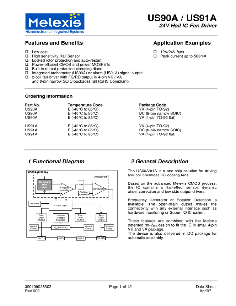
1 Functional Diagram
2 General Description
The US90A/91A is a one-chip solution for driving
two-coil brushless DC cooling fans.
Based on the advanced Melexis CMOS process,
the IC contains a Hall-effect sensor, dynamic
offset correction and low side output drivers.
Frequency Generator or Rotation Detection is
available. The open-drain output makes the
connectivity with any external interface such as
hardware monitoring or Super I/O IC easier.
These features are combined with the Melexis
patented no-VDD design to fit the IC in small 4-pin
VK and VA package.
The device is also delivered in DC package for
automatic assembly.
390109026302
Rev 002
Page 1 of 12
Data Sheet
Apr/07
US90A / US91A
24V Hall IC Fan Driver
Table of Contents
1 Functional Diagram ........................................................................................................ 1
2 General Description........................................................................................................ 1
3 Glossary of Terms .......................................................................................................... 3
4 Absolute Maximum Ratings ........................................................................................... 3
5 Pin Definitions and Descriptions................................................................................... 3
6 General Electrical Specifications .................................................................................. 4
7 Magnetic Specifications ................................................................................................. 4
8 Driver Output vs Magnetic Pole..................................................................................... 4
9 Detailed General Description ......................................................................................... 5
10 Unique Features............................................................................................................ 5
11 Performance Graphs .................................................................................................... 6
11.1 RDSON vs TJ...................................................................................................................................................................... 6
11.2 RDSON vs VDD .................................................................................................................................................................. 6
11.3 Magnetic parameters vs TJ .................................................................................................................................. 6
11.4 Magnetic parameters vs VDD............................................................................................................................... 6
11.5 IDD vs TJ ............................................................................................................................................................................. 6
11.6 IDD vs VDD ......................................................................................................................................................................... 6
11.7 VOL vs TJ ........................................................................................................................................................................... 7
11.8 Power Dissipation vs. TA ....................................................................................................................................... 7
12 Application Information................................................................................................ 7
12.1 Typical application with pull-up resistor..................................................................... 7
12.2 Configuration for reverse voltage / ground hot-switch protection and enhanced ESD
module protection ............................................................................................................. 7
13 Application Comments ................................................................................................. 7
14 Standard information regarding manufacturability of Melexis products with
different soldering processes........................................................................................... 8
15 ESD Precautions ........................................................................................................... 8
16 Package Information..................................................................................................... 9
16.1 VK Package Information (4-pin TO92)......................................................................................................... 9
16.2 DC Package Information (8-pin narrow SOIC) ..................................................................................... 10
16.3 VA Package Information (4-pin TO92 flat) .............................................................................................. 11
17 Disclaimer.................................................................................................................... 12
390109026302
Rev 002
Page 2 of 12
Data Sheet
Apr/07
US90A / US91A
24V Hall IC Fan Driver
3 Glossary of Terms
Two-coil fan
MilliTesla (mT), Gauss
VDD
IDD
Peak output current
Continuous output current
Locked rotor
FG
RD
LFPM
A fan with two-coil windings where current alternates from 1 coil to the other
depending on the direction of the magnetic field.
Units of magnetic flux density :
1mT = 10 Gauss
Voltage on the coils common node.
Current supplying the chip which flows through the coil connected to the
switched off output driver.
The current flowing in the coil at start-up, only limited by the coil resistance
RCOIL and the output driver resistance RDSON.
The current flowing in the coil when the fan is spinning normally.
The state when the fan stopped spinning due to mechanical blockage.
Frequency generator or tachometer output
Rotation detection or alarm output
Linear Feet Per Minute – Unit of airflow velocity
4 Absolute Maximum Ratings
Parameter
Symbol
Fan Supply Voltage
VDD
Peak Output Current
IOUTp
Continuous Output Current
IOUTc
FG / RD Output Current
IFG (RD)
Operating Temperature Range
TA
Junction Temperature
TJ
Storage Temperature Range
TS
Magnetic Flux Density
B
Table 1: Absolute maximum ratings
Value
30
500
250
20
-40 to 85
125
-55 to 150
Unlimited
Units
V
mA
mA
mA
°C
°C
°C
mT
Exceeding the absolute maximum ratings may cause permanent damage. Exposure to absolute-maximumrated conditions for extended periods may affect device reliability.
5 Pin Definitions and Descriptions
Pin Name Pin number (VK) Pin number (DC) Pin number (VA)
FG (RD)
1
1
1
OUT1
2
2
2
OUT2
3
4
4
GND
4
3
3
5, 6, 7, 8
Table 2: Pin definitions and descriptions US90A (US91A)
390109026302
Rev 002
Page 3 of 12
Function
FG (RD) open drain output signal
Open Drain Coil Driver 1
Open Drain Coil Driver 2
Ground pin
Not Connected
Data Sheet
Apr/07
US90A / US91A
24V Hall IC Fan Driver
6 General Electrical Specifications
o
DC Operating Parameters TA = 25 C, VDD = 24V (unless otherwise specified)
Parameter
Symbol Test Conditions
Fan Supply Voltage
VDD
Operating, RCOIL = 50Ω
Supply Current
IDD
Output Saturation Voltage
VDSON 1,2 IOUT = 150mA
Output Saturation Voltage
VDSON 1,2 IOUT = 250mA
Output Clamp Voltage
VOUT 1,2
FG / RD Output Low Voltage
VOL
IOL = 10mA
FG / RD Output Clamp Voltage
VCLAMP
FG / RD Output Leakage Current ILEAK
VFG (VRD) = 18V
DC Thermal Resistance
RTHja
One-sided PCB, zero LFPM
VK Thermal Resistance
RTHja
One-sided PCB, zero LFPM
VA Thermal Resistance
RTHja
One-sided PCB, zero LFPM
Locked Rotor Period
TON
Locked Rotor Period
TOFF
Output Switching Delay
TDELAY
“Dead time” when both drivers are off
Table 3: General electrical specifications
Min
4.7(1)
Typ
2
375
625
Max
30
4
60
250
500
28
10
150
200
170
0.25
1.5
200
Units
V
mA
mV
mV
V
mV
V
µA
°C/Watt
°C/Watt
°C/Watt
S
S
us
Note 1: The minimal value of VDD should be determined using the following equation: VDD = 4.5V + RCOIL * IDD
7 Magnetic Specifications
o
DC Operating Parameters TA = 25 C, VDD = 24V (unless otherwise specified)
Parameter
Symbol
Test Conditions
Operate point
BOP
Release point
BRP
Hysteresis
BHYST
Table 4: Magnetic specifications
Min
-6
2
Typ
3
-3
6
Max
6
Units
mT
mT
mT
8 Driver Output vs Magnetic Pole
Parameter
Test Conditions
North pole
B < Brp – all packages
South pole
B > Bop - all packages
Table 5: Driver output vs. magnetic pole
OUT1
High
Low
OUT2
Low
High
Note 3: The magnetic pole is applied facing the branded side of the package
390109026302
Rev 002
Page 4 of 12
Data Sheet
Apr/07
US90A / US91A
24V Hall IC Fan Driver
9 Detailed General Description
The US90A/91A is a one-chip solution for driving two-coil brushless DC fans. Based on advanced Melexis
CMOS process, the IC contains a Hall-effect sensor, dynamic offset correction and low side output drivers.
The output drivers OUT1 and OUT2 are fully protected against switching transients. So there is no need for
an external zener diode to cut the high voltage spikes induced by the fan coils.
The US90A has an open-drain integrated tachometer FG output that follows the Hall signal.
In the US91A, the open-drain rotation detection output RD is active low during normal spinning of the motor.
It goes high when the flux switching frequency becomes too low, which means the motor is blocked.
10 Unique Features
The absence of a VDD pin enables the two low side output drivers and FG/RD signal output to fit in a four-pin
VK package. The lack of a VDD pin decreases also the probability to damage the chip due to reverse voltage
connection, using the coil resistance to limit the reverse current. In this condition, the total reverse current is
twice the peak current value of the fan used.
The built-in locked-rotor protection will automatically shut off the coil current when the rotor is mechanically
blocked, or the rotational speed drops below 60 RPM (4-pole rotor magnet). The fan will try to restart every
1.5 seconds until the obstruction is clear. The On / Off cycling reduces the average stall current to 1/7 normal;
this is enough to prevent overheating or damage to most fans. Both the US90A and US91A have this feature.
390109026302
Rev 002
Page 5 of 12
Data Sheet
Apr/07
US90A / US91A
24V Hall IC Fan Driver
11 Performance Graphs
11.1 RDSON vs TJ
11.2 RDSON vs VDD
5
5
VDD = 5V
Tj = -40°C
VDD = 24V
4
Tj = 25°C
4
3
Ron (ohms)
Ron (ohms)
Tj = 125°C
2
1
3
2
1
0
0
-40
-20
0
20
40
60
80
100
120
0
2
4
6
8
10
12
Tj (°C)
11.3 Magnetic parameters vs TJ
16
18
20
22
24
26
28
30
11.4 Magnetic parameters vs VDD
6
6
5
Bop, VDD=5V
Bop, VDD=24V
5
4
Brp, VDD=5V
Brp, VDD=24V
4
3
3
2
2
Magnetic field (mT)
Magnetic field (mT)
14
VDD (Volts)
1
0
-1
-2
Bop, Tj=125°C
Brp, Tj=125°C
Brp, Tj=-40°C
1
0
-1
-2
-3
-3
-4
-4
-5
-5
-6
Bop, Tj=25°C
Brp, Tj=25°C
Bop, Tj=-40°C
-6
-40
-20
0
20
40
60
80
100
120
0
2
4
6
8
10
12
Tj (°C)
14
16
18
20
22
24
26
28
30
VDD (Volts)
11.5 IDD vs TJ
11.6 IDD vs VDD
4
4
3.5
3.5
Tj = -40°C
Tj = 25°C
3
3
Tj = 125°C
VDD = 5V
2.5
VDD = 24V
IDD (mA)
IDD (mA)
2.5
2
1.5
2
1.5
1
1
0.5
0.5
0
0
-40
-20
0
20
40
60
80
100
120
0
Tj (°C)
390109026302
Rev 002
2
4
6
8
10
12
14
16
18
20
22
24
26
28
30
VDD (Volts)
Page 6 of 12
Data Sheet
Apr/07
US90A / US91A
24V Hall IC Fan Driver
11.7 VOL vs TJ
11.8 Power Dissipation vs. TA
0.8
0.4
0.3
VDD=5V ; Iol=10mA
VDD=24V ; Iol=10mA
0.2
VK - RTH = 200°C/W - PDMAX = 500mW
TA = 25°C
0.7
Allowable Power Dissipation (W)
FG/RD Output Saturation Voltage (Volts)
0.5
VA - RTH = 170°C/W - PDMAX = 588mW
DC - RTH = 150°C/W - PDMAX = 666mW
0.6
0.5
0.4
T A max = 85°C
0.3
0.2
0.1
0.1
TJ max = 125°C
0
0
-40
-20
0
20
40
60
80
100
120
-40
-20
0
20
40
60
80
100
120
140
Ta (°C)
Tj (°C)
12 Application Information
12.1 Typical application with pull-up
resistor
12.2 Configuration for reverse voltage /
ground hot-switch protection and
enhanced ESD module protection
13 Application Comments
Figure 12.2 shows the application including several external protections.
The diode DREVPROT best protects the chip and fan coils for reverse voltage condition.
The capacitor CBYPASS is recommended if the supply ground may be disconnected while running even though
the positive supply point is still connected. This capacitor provides a path to ground for the remaining energy
in the coil which has to be evacuated. Without it, the energy can flow from OUT1/OUT2 to the FG/RD driver,
without any limitation and may cause EOS damage.
Its value has to be tuned depending on the coils characteristics. Bigger inductance requires bigger capacitor.
The no-VDD design enables ESD protection at fan module level to be easily improved. The fan coils prevent
and filter fast current stress on OUT1 and OUT2, resulting in better ESD protection. Adding the optional
capacitor COUT enhances the ESD protection of the logic output. Hence, the fan module is able to withstand
ESD stress at relatively high value without damage.
390109026302
Rev 002
Page 7 of 12
Data Sheet
Apr/07
US90A / US91A
24V Hall IC Fan Driver
14 Standard information regarding manufacturability of Melexis
products with different soldering processes
Our products are classified and qualified regarding soldering technology, solderability and moisture sensitivity
level according to following test methods:
Reflow Soldering SMD’s (Surface Mount Devices)
•
•
•
IPC/JEDEC J-STD-020
Moisture/Reflow Sensitivity Classification for Nonhermetic Solid State Surface Mount Devices
(classification reflow profiles according to table 5-2)
EIA/JEDEC JESD22-A113
Preconditioning of Nonhermetic Surface Mount Devices Prior to Reliability Testing
(reflow profiles according to table 2)
Melexis Working Instruction 341901308
Wave Soldering SMD’s (Surface Mount Devices) and THD’s (Through Hole Devices)
•
•
•
EN60749-20
Resistance of plastic- encapsulated SMD’s to combined effect of moisture and soldering heat
EIA/JEDEC JESD22-B106 and EN60749-15
Resistance to soldering temperature for through-hole mounted devices
Melexis Working Instruction 341901309
Iron Soldering THD’s (Through Hole Devices)
•
•
EN60749-15
Resistance to soldering temperature for through-hole mounted devices
Melexis Working Instruction 341901309
Solderability SMD’s (Surface Mount Devices) and THD’s (Through Hole Devices)
•
•
EIA/JEDEC JESD22-B102 and EN60749-21
Solderability
Melexis Working Instruction 3304312
For all soldering technologies deviating from above mentioned standard conditions (regarding peak
temperature, temperature gradient, temperature profile etc) additional classification and qualification tests
have to be agreed upon with Melexis.
The application of Wave Soldering for SMD’s is allowed only after consulting Melexis regarding assurance of
adhesive strength between device and board.
For more information on the lead free topic please see quality page at our website:
http://www.melexis.com/quality.aspx
15 ESD Precautions
Electronic semiconductor products are sensitive to Electro Static Discharge (ESD).
Always observe Electro Static Discharge control procedures whenever handling semiconductor products.
390109026302
Rev 002
Page 8 of 12
Data Sheet
Apr/07
US90A / US91A
24V Hall IC Fan Driver
16 Package Information
16.1 VK Package Information (4-pin TO92)
1.55+/-0.10
4.20+/-0.10
0.73+/-0.10
0.46 -+0.02
0.03
+2
5° -1 (2X)
Notes:
1. All dimensions are in millimeters
2. Package dimension exclude molding flash.
Mold flash shall not exceed 0.127mm.
3. To preserve reliability, it is recommended to
have total lead length equal to 2.5mm minimum,
measured from the package line.
4. VK package is a pin through-hole package,
hence adapted for wave soldering process.
A reflow soldering process is not recommended
with VK package as it may seriously affect
device reliability.
10.50+/-0.30
0.00
0.20
3°+2 (2X)
2.5 min
see note 3
1.42+/-0.10
E.D.M Process Surface Ro1.6~2.4um
3.65+/-0.10
5.22+/-0.10
Marking:
1st Line : US90A (US91A) - Name of the device
2nd Line : xxxx - Assembly lot number (4 last digits)
0.38+/-0.03
1.27+/-0.03
0.38+/-0.03
3.81+/-0.03
5° +2
-1
(2X)
0.30+/-0.10
(2X)
3°+2
(2X)
Hall plate location
2.25
0.52
Notes:
1.05
1. All dimensions are in millimeters
2. Typical values
390109026302
Rev 002
Page 9 of 12
Data Sheet
Apr/07
US90A / US91A
24V Hall IC Fan Driver
3.81
3.99
1.52
1.72
1.95
1.37
1.57
5.80
6.20
16.2 DC Package Information (8-pin narrow SOIC)
390109026302
Rev 002
Page 10 of 12
Data Sheet
Apr/07
US90A / US91A
24V Hall IC Fan Driver
16.3 VA Package Information (4-pin TO92 flat)
1x45°(REF)
1.10
1.20
5.38+/-0.05
5.16+/-0.08
4.30+/-0.20
0.61
0.66
0.24
0.29
5°
Notes:
1. All dimensions are in millimeters
2. Package dimension exclude end flash
5°(2X)
45°(TYP)
Marking:
0.30+/-0.05
Top Side:
1 max
1st Line : US90A (US91A) - Name of the device
0.40
0.60
2nd Line : xxxxxx - Assembly lot number (last 6 digits)
Bottom Side:
yyww : yy = year
ww = week
0.40+/-0.05
1.27+/-0.05
+0.06
0.25 - 0.07
3.81+/-0.05
5°(2x)
45°(2x)
5°(2x)
2.69
Hall plate location
0.33
Notes:
1. All dimensions are in millimeters
2. Typical values
390109026302
Rev 002
Page 11 of 12
Data Sheet
Apr/07
US90A / US91A
24V Hall IC Fan Driver
17 Disclaimer
Devices sold by Melexis are covered by the warranty and patent indemnification provisions appearing in its
Term of Sale. Melexis makes no warranty, express, statutory, implied, or by description regarding the
information set forth herein or regarding the freedom of the described devices from patent infringement.
Melexis reserves the right to change specifications and prices at any time and without notice. Therefore, prior
to designing this product into a system, it is necessary to check with Melexis for current information. This
product is intended for use in normal commercial applications. Applications requiring extended temperature
range, unusual environmental requirements, or high reliability applications, such as military, medical lifesupport or life-sustaining equipment are specifically not recommended without additional processing by
Melexis for each application.
The information furnished by Melexis is believed to be correct and accurate. However, Melexis shall not be
liable to recipient or any third party for any damages, including but not limited to personal injury, property
damage, loss of profits, loss of use, interrupt of business or indirect, special incidental or consequential
damages, of any kind, in connection with or arising out of the furnishing, performance or use of the technical
data herein. No obligation or liability to recipient or any third party shall arise or flow out of Melexis’ rendering
of technical or other services.
© 2002 Melexis NV. All rights reserved.
For the latest version of this document, go to our website at
www.melexis.com
Or for additional information contact Melexis Direct:
Europe and Japan:
Phone: +32 1367 0495
E-mail: sales_europe@melexis.com
All other locations:
Phone: +1 603 223 2362
E-mail: sales_usa@melexis.com
ISO/TS 16949 and ISO14001 Certified
390109026302
Rev 002
Page 12 of 12
Data Sheet
Apr/07


