04054686 - Department of Electronics
advertisement

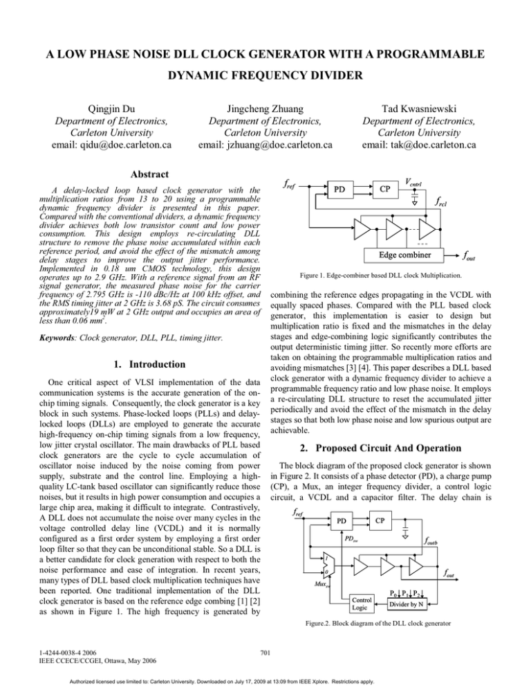
A LOW PHASE NOISE DLL CLOCK GENERATOR WITH A PROGRAMMABLE DYNAMIC FREQUENCY DIVIDER Qingjin Du Department of Electronics, Carleton University email: qidu@doe.carleton.ca Jingcheng Zhuang Department of Electronics, Carleton University email: jzhuang@doe.carleton.ca Abstract A delay-locked loop based clock generator with the multiplication ratios from 13 to 20 using a programmable dynamic frequency divider is presented in this paper. Compared with the conventional dividers, a dynamic frequency divider achieves both low transistor count and low power consumption. This design employs re-circulating DLL structure to remove the phase noise accumulated within each reference period, and avoid the effect of the mismatch among delay stages to improve the output jitter performance. Implemented in 0.18 um CMOS technology, this design operates up to 2.9 GHz. With a reference signal from an RF signal generator, the measured phase noise for the carrier frequency of 2.795 GHz is -110 dBc/Hz at 100 kHz offset, and the RMS timing jitter at 2 GHz is 3.68 pS. The circuit consumes approximately19 mW at 2 GHz output and occupies an area of less than 0.06 mm2. Keywords: Clock generator, DLL, PLL, timing jitter. 1. Introduction One critical aspect of VLSI implementation of the data communication systems is the accurate generation of the onchip timing signals. Consequently, the clock generator is a key block in such systems. Phase-locked loops (PLLs) and delaylocked loops (DLLs) are employed to generate the accurate high-frequency on-chip timing signals from a low frequency, low jitter crystal oscillator. The main drawbacks of PLL based clock generators are the cycle to cycle accumulation of oscillator noise induced by the noise coming from power supply, substrate and the control line. Employing a highquality LC-tank based oscillator can significantly reduce those noises, but it results in high power consumption and occupies a large chip area, making it difficult to integrate. Contrastively, A DLL does not accumulate the noise over many cycles in the voltage controlled delay line (VCDL) and it is normally configured as a first order system by employing a first order loop filter so that they can be unconditional stable. So a DLL is a better candidate for clock generation with respect to both the noise performance and ease of integration. In recent years, many types of DLL based clock multiplication techniques have been reported. One traditional implementation of the DLL clock generator is based on the reference edge combing [1] [2] as shown in Figure 1. The high frequency is generated by fref Tad Kwasniewski Department of Electronics, Carleton University email: tak@doe.carleton.ca CP PD Vcntrl frcl fout Edge combiner Figure 1. Edge-combiner based DLL clock Multiplication. combining the reference edges propagating in the VCDL with equally spaced phases. Compared with the PLL based clock generator, this implementation is easier to design but multiplication ratio is fixed and the mismatches in the delay stages and edge-combining logic significantly contributes the output deterministic timing jitter. So recently more efforts are taken on obtaining the programmable multiplication ratios and avoiding mismatches [3] [4]. This paper describes a DLL based clock generator with a dynamic frequency divider to achieve a programmable frequency ratio and low phase noise. It employs a re-circulating DLL structure to reset the accumulated jitter periodically and avoid the effect of the mismatch in the delay stages so that both low phase noise and low spurious output are achievable. 2. Proposed Circuit And Operation The block diagram of the proposed clock generator is shown in Figure 2. It consists of a phase detector (PD), a charge pump (CP), a Mux, an integer frequency divider, a control logic circuit, a VCDL and a capacitor filter. The delay chain is fref CP PD PDsw foutb 1 fout 0 Muxsw Control Logic P0 P1 P2 Divider by N Figure.2. Block diagram of the DLL clock generator 1-4244-0038-4 2006 IEEE CCECE/CCGEI, Ottawa, May 2006 701 Authorized licensed use limited to: Carleton University. Downloaded on July 17, 2009 at 13:09 from IEEE Xplore. Restrictions apply. configured as a VCO or a VCDL depending on the control signal of the Mux, i.e. when the control signal is 0, the rising edge of the reference signal fref is propagated in the delay chain, and when the control signal is changed to 1, this rising edge circulates in the delay chain which is essentially a VCO. After N output cycles, where N is determined by the division ratio of the divider, this rising edge is taken out and compared D D Ck N1 N2 N2 Ck N1 Ck P3 P3 P2 Ck P2 x P1 P1 x N3 N3 Ck (1) (2) (3) (4) (1) (2) (3) (4) Q Ck Q Q Q Figure 4. Dynamic divide-by-2 divider Figure 4. Dynamic divide-by-2 divider fref 3 Ck D foutb y Ck Figure 3. The system error when the loop is in lock with the phase of next rising reference edge with a phase detector, by which UP and DN signals are generated to tune the VCO frequency to the desired value with the aid of a charge pump and a loop filter. Figure 3 shows the operation of the clock generator with an example of N = 6. On the 6th falling edge, one the control logic output MUXsw goes high according to the information from the divider output. The MUX is set to 0, and the reference is connected to the VCDL. The 6th falling edge is inversed to the 6th rising edge after passing the VCDL and its phase is compared with the phase of the rising reference edge just injected as shown in the dashed arrows in Figure 3. After the reference edge is injected, the divider starts to count again, and the injected rising reference edge is inversed after a VCDL delay, appearing as the first falling edge. In the mean time, the MUX is set back to 1, and the injected reference edge circulates in the VCO until the rising edge of MUXsw comes again. 3. Circuit Implementation 3.1. 3-bit Programmable Dynamic Frequency Divider To implement the 3-bit dynamic frequency divider, a dynamic divide-by-2 divider is firstly considered. Figure 4 shows the schematic of the divide-by-2 divider. It consists of 3 PMOS transistors labeled as P1, P2, and P3 and 3 NMOS transistors labeled as N1, N2 and N3. Since the current switching of the three pairs of PMOS and NMOS transistors with drains connected together, depends on the driving ability, the transistor sizing in this type of DFF is very important. For equal driving ability of each transistor pair, the ratio of the W/L of PMOS to that of the NMOS transistor is approximately 2.5. If the size ratio is larger than 2.5 (for better results, the size ratio can be much larger than 2.5), the PMOS transistor charges up the node more than N2 discharges it, and the logic level of the output voltage is determined by the gate voltage of PMOS transistor. Similarly, if the ratio is less than 2.5, the NMOS transistor determines the logic level of the output node. Accordingly, the circuit is connected in a toggle configuration for the sake of facilitating the sizing D x Q 0.5 Ck y x 3 Ck Ck D 3 x Q (2). DP2 < DN2 (1). DP1 > DN1 y Ck 1.5 Ck D 2 y Q 2 (3). DP3 < DN3 Ck x 0.5 Q (4). DP1 > DN1 Figure 5. Transistor sizing of the dynamic DFF in a toggle connection consideration. The desired timing wave of the clock signal Ck and the output Q is shown in Figure 4 and the detailed operation is illustrated in Figure 5. In the pre-charge phase labeled as (1) in Figure 5, before the falling edge of Ck arrives, Ck is high and Q is low, the circuit configuration is the same as in the evaluation phase (4), where node x is discharged to low. Since the driving ability of P1 is larger than N1, y is high. On the falling edge of Ck, N1, N2 is cutoff. This connection change is highlighted in the dashed line or X, which means the transistor is connected or cutoff in the previous phase. P1 is still connected at this point, so Q is charged up more quickly than node x is charged up, thereby N1 is cutoff. Therefore in phase (1), x is low while y and Q bar is high. For the evaluation phase (2), where N1 and N2 are connected on the Ck rising edge, both P2 and N2 is connected, and node y is discharged immediately, which turns on P2. For the desired operation, the voltage on node x needs to be low, and the driving ability of N2 needs to be larger than that of P2, so the transistor sizing ratio should be smaller than 2.5. Accordingly, N3 is still cutoff, and Q keeps high. Similarly, the driving ability of N3 should be larger than P3, and the driving ability of P1 should be larger than that of N1. The transistor sizes are labeled in the circuit. One of the advantages of this structure is that it uses fewer transistors. For the more conventional structure, the source coupled logic (SCL) circuit typically consists of 18 transistors and a few of extra transistors as output buffer. With the dynamic structure, the power consumption is reduced due to 702 Authorized licensed use limited to: Carleton University. Downloaded on July 17, 2009 at 13:09 from IEEE Xplore. Restrictions apply. the reduced capacitive load. The 2/3 divider is shown in Figure 6. It embodies two DFF described above, one OR gate and one NOR gates. For the normal mode operation, when mode = 1, the output Q of DFF1 is always 0 and DFF2 is in a toggle configuration and works as a divide-by-2 divider. When mode = 0, DFF2 remains high for an extra clock cycle before setting back to 0 and toggles again, and at the same time, signal mode is set back to 1 to prevent extra pulses from being swallowed. The transistor level schematic of the 2/3 divider is shown in Figure 7. The two DFF is shown in the shaded region. With the extended true-single-phase-clock (E-TSPC) logic employed in the divider [5], the power consumption is reduced due to the less number of transistors, and the interconnections among the transistors are much shorter, all of which contributes to low power dissipation and high operating frequency. Another advantage is that this structure allows embedding some logic functions. By simply adding one additional PMOS transistor reset In A 2/3 divider B 2/3 divider 2/3 divider Out Control Qualifier P0 P1 P2 Figure.8. Block diagram of divide-by-N divider mod DFF1 DFF2 D Q out D Q RQ RQ in Figure 9. Simulated operation of the divide-by-N divider reset consumption. The three control signals P0, P1, and P2 programs the multiplication ratio which can be calculated as Fig.6. Block diagram of divide-by-2, 3 divider mod a c N = e In b Out d reset 2 i ⋅ Pi + 8 (1) i=o D Q i=2 ∑ reset Fig.7. Schematic of divide-by-2,3 divider labeled ‘a’ parallel to the PMOS transistor whose drain is the input of the D-FF, the NOR gate formed. Similarly, the OR gate is formed by adding one NMOS transistor b with the drain connected to one output of DFF1. The reset circuit is only added to DFF2 since as long as DFF2 generates the final divided output. To ensure the correct reset, two PMOS transistors labeled as ‘c’ and ‘e’, and one NMOS transistor labeled as ‘d’ are added as shown in the figure. Compared with conventional 2/3 dividers, this structure uses less number of transistors and thus resulting in a compact circuit. By cascading three 2/3 dividers with a control qualifier consisting of three NOR gates, the divide-by-N divider is formed as shown in Figure 8. The asynchronous structure of the divide-by-N divider allows high speed and reduced power From the equation, the frequency division ratios are integers from 8 to 15. Due to the delay of the circuit, the actual multiplication ratio of this clock generator is from 13 to 20. To verify the functionality of the divider, simulation results are obtained from HPICE simulation. Figure 9 shows the operation of the divide-by-N divider. The simulation takes N = 11, P0P1P2 = ‘110’ as an example and the divider is tested alone. By feeding back the three outputs, A, B and out, the first and the second stage divide-by-2,3 dividers divide by 3, while the last stage divides by 2 due to P2 = 0. 3.2. Phase Detector and Charge Pump The phase detector is based on a conventional tri-state phase detector consists of two DFFs. It is controlled by an enable signal PDsw, coming from the control logic. When PDsw is high, the signal DN goes high at rising edge of frcl. Similar to a conventional PFD, UP and DN are reset right after both are high. In addition, the signal UP is reset at falling edge of PDsw to ensure the PFD compares the correct edges so that the lock can be guaranteed without initialization. With the aid of a charge pump and a loop filter, two output signals UP and DN tune the delay of the delay line in a direction to reduce the 703 Authorized licensed use limited to: Carleton University. Downloaded on July 17, 2009 at 13:09 from IEEE Xplore. Restrictions apply. phase error. 3.3. Control logic, VCDL and Mux The control logic ordinates the operation of the PD, the Mux and the divider, and synchronize the loop with the reference frequency. It generates timing signals for controlling these blocks by enabling the phase detector and switching the Mux. The divider is reset once the counting-to-N action is finished and the reference edge is switched into the VCDL. An inverter-based VCDL is used in this design. Its propagation delay is controlled by two bias voltages, which is derived from the control signal Vcntrl. When the Mux selects 0, the reference is injected and when the Mux selects 1, the VCDL works as a VCO and the injected reference edge circulates in the VCDL for N cycles with the clock frequency as: 1 (2) f = Figure 10. Measured cycle-to-cycle timing jitter at 2 GHz 2T where T is the VCDL delay. This selection action is periodic and the phase noise accumulated over N-1 output cycles are zeroed at the reference frequency. MEASUREMENT RESULTS The circuit is implemented in CMOS 0.18μm technology and tested with a synthesized reference signal from an RF signal generator. Figure10 shows the jitter histogram. At the output frequency of 2 GHz, the measured cycle-to-cycle RMS edge jitter is 3.68 pS with the division ratio of N=19. The measured phase noise at a carrier frequency of 2.795 GHz is approximately -119 dBc/Hz at 1MHz offset, and -110 dBc/Hz at 100 kHz offset as shown in Figure 11. With the division ratios from 13 to 20, the output frequencies from 900 MHz to 2.9 GHz are obtained. The circuit consumes 19 mW at 2 GHz, and the active region including the on chip loop capacitor is 0.06 mm2. 4. Conclusions A DLL clock generator with a 3-bit programmable dynamic frequency divider is presented in this paper. Multiple output frequencies are obtained by employing the dynamic programmable frequency divider with the division ratios of 13 to 20. The circuit employs a re-circulating DLL structure for improving phase noise performance, which is confirmed by the measured results. Acknowledgements The authors would like to thank Canadian Microelectronic Corporation (CMC) for the chip fabrication. Financial support of Government of Ontario and NSERC is also gratefully acknowledged. Figure 11. Measured phase noise at 2.795GHz References [1] David J.Foley, "CMOS DLL-Based 2-V 3.2-ps Jitter 1GHz Clock Synthesizer and Temperature-Compensated Tunable Oscillator", IEEE Journal of Solid State Circuits, Vol. 36, pp417-423, March 2001. [2] Chua-Chin Wang, Yih-Long Tseng, et al, "A 1.2 GHz Programmable DLL-Based Frequency Multiplier for Wireless Applications", IEEE VLSI Systems, Vol. 12 No.12, pp1377-1381, Dec 2004. [3] Ramin Farjad-Rad, William Dally, et al, "A Low-Power Multiplying DLL for Low-Jitter Multigigaherz Clock Generation", IEEE Journal of Solid State Circuit, Vol. 37, pp1804-1811, Dec 2002,. [4] Gu-Yeon Wei, John T. Stonick, et al "A 500MHz MP/DLL Clock Generator for a 5Gb/S Backplane Transceiver in 0.25um CMOS", IEEE International Solid State Circuit Conference, Feb 2003. [5] J. Navarro Soares, Jr,.and W, A. M. Van Noije, “A 1.6GHz Dual Modulus Prescaler Using the Extended TrueSingle-Phase-Clock CMOS circuit Techique (E-TSPC)”, IEEE Journal of Solid State Circuit, Vol.34, NO.1, January 1999. 704 Authorized licensed use limited to: Carleton University. Downloaded on July 17, 2009 at 13:09 from IEEE Xplore. Restrictions apply.


